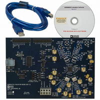
AD9958/PCBZ Analog Devices Inc, AD9958/PCBZ Datasheet
AD9958/PCBZ
Specifications of AD9958/PCBZ
Available stocks


Related parts for AD9958/PCBZ


AD9958/PCBZ Summary of contents
Page 1
XTAL BUFFER/XTAL OSCILLATOR J9 REF_CLK BALUN MULTIPLIER J13 SYNC_CLK J11 SYNC_IN J12 SYNC_OUT FEATURES Full-featured evaluation board for the AD9958 PC evaluation software for control and measurement of the AD9958 USB interface Graphic user interface (GUI) software with frequency sweep ...
Page 2
AD9958/PCB TABLE OF CONTENTS Evaluation Board Block Diagram................................................... 1 Features .............................................................................................. 1 Applications....................................................................................... 1 General Description ......................................................................... 1 Revision History ............................................................................... 2 Evaluation Board Hardware ............................................................ 3 Package Contents.......................................................................... 3 Requirements ................................................................................ 3 Setting up the Evaluation Board................................................. 3 Evaluation ...
Page 3
EVALUATION BOARD HARDWARE PACKAGE CONTENTS The AD9958/PCB kit contains the following items: • AD9958 evaluation board • AD9958/PCB installation software REQUIREMENTS In order to successfully use the evaluation board and run the software, the requirements listed in Table 1 must ...
Page 4
AD9958/PCB MANUAL I/O CONTROL HEADERS EVALUATION BOARD CONTROL USB PORT SDIO Manual I/O Control Headers Provides the interface for communication with the AD9958 when the part is under the control of an external controller (manual control). See Eval Board Control ...
Page 5
EVALUATION BOARD SOFTWARE INSTALLING THE SOFTWARE Follow these steps to install the AD9958 evaluation software. 1. Log on to your PC system with administrative privileges; this is an essential requirement in successfully installing the AD9958 evaluation software. 2. Uninstall any ...
Page 6
AD9958/PCB Windows XP Users 1. Power up the AD9958 evaluation board (see Table 2). 2. Connect the evaluation board to the computer using a USB cable via the USB port. Then, the VBUS LED (CR1 on AD9958 evaluation board) illuminates. ...
Page 7
After the window in Figure 12 appears, click Finish to exit. Figure 12. Once this screen has disappeared, you should notice that the USB Status LED (CR2 on AD9958 evaluation board) is flashing, which indicates that the evaluation board ...
Page 8
AD9958/PCB Status Messages upon Loading Software Once the AD9958 evaluation software has been loaded, a green splash screen appears as shown in Figure 14. The status box within the splash screen gives the status of the AD9958 evaluation software. A ...
Page 9
FEATURE CONTROL WINDOWS Chip Level Control The Chip Level Control window provides control of the features that affect all channels of the AD9958; this window is not channel-specific. The following section describes the options in the Chip ...
Page 10
AD9958/PCB CP Current selects the charge pump current output of the PLL in the Ref Clock Multiplier circuitry. Selecting a higher current output results in the loop locking faster, but there is a trade-off. Increasing this current output also increases ...
Page 11
Channel Control The Channel Control window provides control of the features that affect the AD9958 at a channel-specific level. The following section describes the options of the Channel Control window as they are numerically indexed in ...
Page 12
AD9958/PCB See the DATA LATENCY (PIPELINE DELAY) section in the Specifications table of the AD9958 data sheet for the exact timing delays with and without this feature enabled. Also, refer to the Single Tone Mode-Matched Pipeline Delay section of the ...
Page 13
Channel Output Config The Channel Output Config window configures various output characteristics of the channel(s). Use the Channel 0 and Channel 1 tabs to select which specific channel options to configure. The following section describes the options ...
Page 14
AD9958/PCB In the second field, set the desired output amplitude scale factor (between 0 and 1) of the output signal, where 1 is equivalent to full scale. The Enable ASF check box also represents the starting point of the linear ...
Page 15
Figure 28. In the linear sweep mode of operation, only the first Profile Register field (Frequency 01, Phase 01, or Amplitude 01) is used. It indicates the ending point of the sweep. In Figure 28, the frequency linear sweep begins ...
Page 16
AD9958/PCB Figure 30. To access the Debug window, click View > Debug Window (see Figure 31). Figure 31. DUT I/O Box This dialog box (Figure 32) controls the I/O configuration for the device. Click I/O Reset to send an I/O ...
Page 17
SETUP FILES Introduction The AD9958 can be configured to perform many operations in various combinations. Preconfigured setup files have been included with the AD9958 evaluation software that show the device in all three modes of operation: single tone, modulation, and ...
Page 18
AD9958/PCB Single Tone Mode Open the Single Tone Mode folder to access the single tone mode of operation example setup files. This section discusses the Both Channels on @30_40MHz_RURD enabled.stp file. The Chip Level Control window (Figure 37) from this ...
Page 19
In the Channel Output Config window (Figure 39), Channel 0 has a frequency output of 30 MHz (Frequency 00 box) and Channel 1 an output frequency of 40 MHz. Because the RU/RD operation is enabled, the Enable ASF and Enable ...
Page 20
AD9958/PCB The Chip Level Control window (Figure 41) from this particular setup shows that a 500 MHz System Clock is running, and that a 16- level modulation-no RU/RD is being performed. Notice the Level list located in Modulation Configuration. The ...
Page 21
In the Channel Output Config window (Figure 43), Channel 0 has a frequency output of 3 MHz (Frequency 00 box). When this setup file is loaded, Profile Pin P1 and Profile Pin P3 are pressed as shown in Profile and ...
Page 22
AD9958/PCB The Chip Level Control window (Figure 45) from this particular setup shows that a 500 MHz System Clock is running with RU/RD disabled. The Auto Clear Phase Accumulator and Auto Clear Sweep Accumulator check boxes have been selected in ...
Page 23
In the Channel Output Config window (Figure 47), both channels (Channel 0 and 1) have an output frequency of 10 MHz (Frequency 00 box). The Enable ASF check box is deselected because a linear amplitude sweep is being performed. The ...
Page 24
AD9958/PCB SCHEMATICS P3 43 GND 44 DVDD 45 IO_UPDATE 46 CSB 47 SCLK 48 DVDD_IO 49 SDIO_0 50 SDIO_1 51 SDIO_2 52 SDIO_3 53 SYNC_CLK 54 DVDD 55 GND 56 D0_AGND P3 LOOP_FILT GND PLL/DLL_VDD DVDD PLL/DLL_GND IO_UPDATE CMS CS ...
Page 25
Figure 49. AD9958/PCB Schematic, Page 2 Rev Page AD9958/PCB 05783-052 ...
Page 26
AD9958/PCB R71 GND 1kΩ GND R13 50Ω I/O UPDATE IN J14 I/O UPDATE OUT J15 U12 1 2 74LVC32A I/O_UPDATE_U USB_STATUS 74LVC14A 74LVC14A R16 GND VBUS 800Ω CR1 U7 VBUS D– USB_HDR D+ GND ...
Page 27
ORDERING INFORMATION ORDERING GUIDE Model Description AD9958/PCB Evaluation Board ESD CAUTION ESD (electrostatic discharge) sensitive device. Electrostatic charges as high as 4000 V readily accumulate on the human body and test equipment and can discharge without detection. Although this product ...
Page 28
AD9958/PCB NOTES ©2006 Analog Devices, Inc. All rights reserved. Trademarks and registered trademarks are the property of their respective owners. EB05783-0-1/06(0) Rev Page ...