AD9958/PCBZ Analog Devices Inc, AD9958/PCBZ Datasheet - Page 9
AD9958/PCBZ
Manufacturer Part Number
AD9958/PCBZ
Description
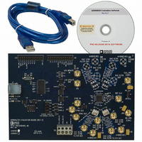
BOARD EVALUATION FOR AD9958
Manufacturer
Analog Devices Inc
Series
AgileRF™r
Specifications of AD9958/PCBZ
Design Resources
Low Jitter Sampling Clock Generator for High Performance ADCs Using AD9958/9858 and AD9515 (CN0109) Phase Coherent FSK Modulator (CN0186)
Main Purpose
Timing, Direct Digital Synthesis (DDS)
Embedded
No
Utilized Ic / Part
AD9958
Primary Attributes
10-Bit DAC, 32-Bit Tuning Word Width
Secondary Attributes
500MHz, Graphical User Interface, 2-Channel
Lead Free Status / RoHS Status
Lead free / RoHS Compliant
Available stocks
Company
Part Number
Manufacturer
Quantity
Price
Company:

Part Number:
AD9958/PCBZ
Manufacturer:
Analog Devices Inc
Quantity:
135


FEATURE CONTROL WINDOWS
Chip Level Control
The Chip Level Control window provides control of the
features that affect all channels of the AD9958; this window is
not channel-specific. The following section describes the
options in the Chip Level Control window as they are
numerically indexed in Figure 17.
1. LOAD and READ
The LOAD and READ buttons are used to send data and
retrieve register settings. All LOAD and READ buttons found in
the evaluation software have the same functionality.
When new data is detected, LOAD flashes orange, indicating
that you need to click LOAD to send the updates to the serial
I/O buffer where they are stored until an I/O update is issued.
The I/O update sends the contents of the serial I/O buffer to
active registers.
I/O updates can be sent manually (Manual I/O Update) or
automatically (Auto I/O Update). By default, the AD9958
evaluation software is set to Auto I/O Update, so that when
LOAD is clicked, an I/O update signal is automatically sent to
the device. If synchronization across channels is desired, use the
Manual I/O Update button. To do this, deselect the Auto I/O
Update box and click the Manual I/O Update button when you
wish to send an I/O update (see Figure 18).
2
3
4
Figure 18.
Figure 17. Chip Level Control Window
Rev. 0 | Page 9 of 28
Click READ to perform a readback of the current state of the
settings and update the GUI with those settings.
2. Clock
Clock allows the user to configure the reference clock path in
the AD9958.
Ref Clock inputs the operating frequency of the external
reference clock or crystal. The maximum reference clock
frequency of the AD9958 is 500 MHz, which is the default
setting of this box. A red outline indicates that the value entered
is out of range (see Figure 19).
Multiplier selects the PLL multiplication factor (4× to 20×) by
which to scale the input frequency. The default setting of this
box is Disabled, indicating that the Ref Clock Multiplier
circuitry is bypassed and the Ref Clock/Crystal input is piped
directly to the DDS core.
Figure 19.
5
6
1
AD9958/PCB
Related parts for AD9958/PCBZ
Image
Part Number
Description
Manufacturer
Datasheet
Request
R

Part Number:
Description:
BOARD EVALUATION FOR AD9958
Manufacturer:
Analog Devices Inc
Datasheet:


Part Number:
Description:
±1.7g Dual-Axis IMEMS Accelerometer Evaluation Board
Manufacturer:
Analog Devices Inc
Datasheet:

Part Number:
Description:
Inertial Sensor Evaluation System
Manufacturer:
Analog Devices Inc
Datasheet:
Part Number:
Description:
Manufacturer:
Analog Devices Inc
Datasheet:
Part Number:
Description:
Manufacturer:
Analog Devices Inc
Datasheet:
Part Number:
Description:
Manufacturer:
Analog Devices Inc
Datasheet:
Part Number:
Description:
Manufacturer:
Analog Devices Inc
Datasheet:
Part Number:
Description:
Manufacturer:
Analog Devices Inc
Datasheet:
Part Number:
Description:
Manufacturer:
Analog Devices Inc
Datasheet:
Part Number:
Description:
Manufacturer:
Analog Devices Inc
Datasheet:
Part Number:
Description:
Manufacturer:
Analog Devices Inc
Datasheet:
Part Number:
Description:
Manufacturer:
Analog Devices Inc
Datasheet: