AD9958/PCBZ Analog Devices Inc, AD9958/PCBZ Datasheet - Page 14
AD9958/PCBZ
Manufacturer Part Number
AD9958/PCBZ
Description
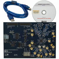
BOARD EVALUATION FOR AD9958
Manufacturer
Analog Devices Inc
Series
AgileRF™r
Specifications of AD9958/PCBZ
Design Resources
Low Jitter Sampling Clock Generator for High Performance ADCs Using AD9958/9858 and AD9515 (CN0109) Phase Coherent FSK Modulator (CN0186)
Main Purpose
Timing, Direct Digital Synthesis (DDS)
Embedded
No
Utilized Ic / Part
AD9958
Primary Attributes
10-Bit DAC, 32-Bit Tuning Word Width
Secondary Attributes
500MHz, Graphical User Interface, 2-Channel
Lead Free Status / RoHS Status
Lead free / RoHS Compliant
Available stocks
Company
Part Number
Manufacturer
Quantity
Price
Company:

Part Number:
AD9958/PCBZ
Manufacturer:
Analog Devices Inc
Quantity:
135


AD9958/PCB
In the second field, set the desired output amplitude scale factor
(between 0 and 1) of the output signal, where 1 is equivalent to
full scale.
The Enable ASF check box also represents the starting point of
the linear amplitude sweep and the first level in amplitude
modulation (ASK). Note that when performing linear
amplitude sweeps, the Enable ASF check box must be left clear.
When using the RU/RD feature, the Enable Auto ASF check
box must be selected. Once the Enable Auto ASF check box has
been selected, the Amplitude Ramp Rate, Amplitude Step
Adjust, and the Load ARR @ I/O Update options are available
(see Figure 25).
Use the Amplitude Ramp Rate field to set the amplitude ramp
rate (ARR) time. This time (entered in μs) can range from a
minimum value of
to a maximum value of
This implies that if the system clock is 500 MHz, the ARR value
can range from 8 ns (minimum) to 2.040 μs (maximum). If the
value entered exceeds the maximum time, a pop-up window
(Figure 26) alerts the user that the value entered will be changed
to the appropriate maximum value.
In the Amplitude Step Adjust drop-down box, select the
amplitude scale factor step size. The default setting of this drop-
down box is 1, indicating that step size is 1 LSB. A selection of
8 means the step size is 8 LSB.
Select Load ARR @ I/O Update to load the contents of the
amplitude ramp rate register into the amplitude ramp rate timer
every time an I/O_UPDATE is sent to the device.
⎛
⎜
⎜
⎝
⎛
⎜
⎜
⎝
⎛
⎜
⎜
⎝
1
1
⎞
⎟
⎟
⎠
⎞
⎟
⎟
⎠
×
×
1
2
(
8
Figure 25.
Figure 26.
)
−1
⎞
⎟
⎟
⎠
Rev. 0 | Page 14 of 28
2. Profile Registers
The AD9958 features up to 16 programmable registers per
channel as shown in Figure 23. Due to certain channel
constraints, however, there are limitations on how the Profile
Registers can be used in some configurations as described in the
Channel Constraint Guidelines section of the AD9958 data sheet.
Use the Profile Registers to enter the information needed for
modulation (FSK, PSK, or ASK) and linear sweep modes of
operation. Upon default, the Profile Registers are configured
for frequency inputs, but these registers can be changed to
intake phase or amplitude information by selecting the desired
modulation type in the Modulation Output Type list in the
Channel Control window. Figure 27 shows how the Profile
Registers appear when phase modulation (PSK) is selected.
When the channel is in the modulation or linear sweep mode of
operation, input the starting frequency in the Frequency 00
field, starting phase in the Phase Offset field, and the starting
amplitude in the Enable ASF field. In modulation mode, use
the Profile Registers to input frequency, phase, or amplitude
information for the level of modulation selected. For instance, if
4-level frequency modulation is selected, input the starting
frequency in the Frequency 00 field, second frequency in the
Frequency 01 field, third frequency in the Frequency 02 field,
and fourth frequency in the Frequency 03 field. An example of
using the Profile Registers for 2-level frequency modulation is
shown in Figure 28. In this configuration, the frequency starts
at 10 MHz and ramps up to 50 MHz.
Figure 27.
Related parts for AD9958/PCBZ
Image
Part Number
Description
Manufacturer
Datasheet
Request
R

Part Number:
Description:
BOARD EVALUATION FOR AD9958
Manufacturer:
Analog Devices Inc
Datasheet:


Part Number:
Description:
±1.7g Dual-Axis IMEMS Accelerometer Evaluation Board
Manufacturer:
Analog Devices Inc
Datasheet:

Part Number:
Description:
Inertial Sensor Evaluation System
Manufacturer:
Analog Devices Inc
Datasheet:
Part Number:
Description:
Manufacturer:
Analog Devices Inc
Datasheet:
Part Number:
Description:
Manufacturer:
Analog Devices Inc
Datasheet:
Part Number:
Description:
Manufacturer:
Analog Devices Inc
Datasheet:
Part Number:
Description:
Manufacturer:
Analog Devices Inc
Datasheet:
Part Number:
Description:
Manufacturer:
Analog Devices Inc
Datasheet:
Part Number:
Description:
Manufacturer:
Analog Devices Inc
Datasheet:
Part Number:
Description:
Manufacturer:
Analog Devices Inc
Datasheet:
Part Number:
Description:
Manufacturer:
Analog Devices Inc
Datasheet:
Part Number:
Description:
Manufacturer:
Analog Devices Inc
Datasheet: