EVAL6206PD STMicroelectronics, EVAL6206PD Datasheet - Page 8
EVAL6206PD
Manufacturer Part Number
EVAL6206PD
Description
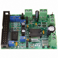
EVAL BOARD FOR L6206 SERIES
Manufacturer
STMicroelectronics
Datasheet
1.L6206N.pdf
(23 pages)
Specifications of EVAL6206PD
Mfg Application Notes
PractiSPIN AppNote
Design Resources
EVAL6206PD/6206PD Gerber Files EVAL6206PD Schematic/Bill of Materials
Main Purpose
Power Management, H Bridge Driver (Internal FET)
Embedded
No
Utilized Ic / Part
L6206
Primary Attributes
2 H-Bridge, 8 ~ 52V Output, Use with PractiSPIN
Secondary Attributes
Temperature Protection, Adjustable Current Limit
Applications
Motor Control
Processor To Be Evaluated
L6206PD
For Use With
497-4138 - EVALUATION BOARD PRACTISPIN
Lead Free Status / RoHS Status
Contains lead / RoHS non-compliant
Other names
497-4135


L6206
CIRCUIT DESCRIPTION
POWER STAGES and CHARGE PUMP
The L6206 integrates two independent Power MOS
Full Bridges. Each Power MOS has an Rd-
son=0.3ohm (typical value @ 25°C), with intrinsic
fast freewheeling diode. Cross conduction protection
is achieved using a dead time (td = 1 s typical) be-
tween the switch off and switch on of two Power MOS
in one leg of a bridge.
Using N Channel Power MOS for the upper transis-
tors in the bridge requires a gate drive voltage above
the power supply voltage. The Bootstrapped (Vboot)
supply is obtained through an internal Oscillator and
few external components to realize a charge pump
circuit as shown in Figure 3. The oscillator output
(VCP) is a square wave at 600kHz (typical) with 10V
amplitude. Recommended values/part numbers for
the charge pump circuit are shown in Table1.
Table 1. Charge Pump External Components
Figure 3. Charge Pump Circuit
LOGIC INPUTS
Pins IN1
CMOS and uC compatible logic inputs. The internal
structure is shown in Fig. 4. Typical value for turn-on
and turn-off thresholds are respectively Vthon=1.8V
and Vthoff = 1.3V.
Pins EN
Overcurrent and Thermal protection by connecting
them respectively to the outputs OCD
which are open-drain outputs. If that type of connec-
tion is chosen, some care needs to be taken in driving
8/23
C
C
R
D1
D2
BOOT
P
P
A
A
VCP
, IN2
and EN
Values
D1
R
C
P
P
D2
A
, IN1
VBOOT
B
are commonly used to implement
C
B
BOOT
, IN2
VS
B
220nF
10nF
100
1N4148
1N4148
A
, EN
VS
B
A
and EN
D01IN1328
A
V
S
and OCD
B
are TTL/
B
,
these pins. Two configurations are shown in Fig. 5
and Fig. 6. If driven by an open drain (collector) struc-
ture, a pull-up resistor R
connected as shown in Fig. 5. If the driver is a stan-
dard Push-Pull structure the resistor R
pacitor C
resistor R
2.2k to 180K . Recommended values for R
C
mation on selecting the values is found in the Over-
current Protection section.
Figure 4. Logic Inputs Internal Structure
Figure 5. EN
Figure 6. EN
TRUTH TABLE
X
High Z
COLLECTOR
PUSH-PULL
EN
OUTPUT
OUTPUT
OPEN
EN
H
H
H
H
L
are respectively 100K
= Don't care
EN
= High Impedance Output
Driving
EN
INPUTS
are connected as shown in Fig. 6. The
R
should be chosen in the range from
A
A
IN1
EN
5V
X
H
H
L
L
and EN
and EN
C
R
EN
EN
C
PROTECTION
EN
OCD
OCD
ESD
EN
A
EN
B
or OCD
A
B
A
IN2
EN
X
H
H
or EN
or OCD
A
L
L
Pins Open Collector
Pins Push-Pull Driving
or EN
and a capacitor C
B
B
5V
and 5.6nF. More infor-
B
B
D01IN1329
High Z
OUT1
GND
GND
Vs
Vs
OUTPUTS
EN
and the ca-
5V
5V
High Z
OUT2
GND
GND
D02IN1355
EN
D02IN1356
Vs
Vs
EN
and
are
Related parts for EVAL6206PD
Image
Part Number
Description
Manufacturer
Datasheet
Request
R

Part Number:
Description:
ENERCHIP CC EVAL KIT
Manufacturer:
Cymbet Corporation
Datasheet:

Part Number:
Description:
BOARD EVAL FOR AD976
Manufacturer:
Analog Devices Inc
Datasheet:

Part Number:
Description:
BOARD EVAL FOR ADXL345
Manufacturer:
Analog Devices Inc
Datasheet:

Part Number:
Description:
ENERCHIP CC SEH EVAL KIT
Manufacturer:
Cymbet Corporation
Datasheet:

Part Number:
Description:
ENERCHIP EP ENERGY HARVEST EVAL
Manufacturer:
Cymbet Corporation
Datasheet:

Part Number:
Description:
EVAL BOARD FOR TW6864-LB2-GR
Manufacturer:
Intersil
Datasheet:
Part Number:
Description:
EVAL BOARD FOR TW8816-LB3-GR
Manufacturer:
Intersil
Datasheet:
Part Number:
Description:
EVAL BOARD FOR TW8817-TA3-GRS
Manufacturer:
Intersil
Datasheet:

Part Number:
Description:
EVALUATION MODULE FOR ADUM4160
Manufacturer:
Analog Devices Inc
Datasheet:

Part Number:
Description:
BOARD EVALUATION ADCMP581BCP
Manufacturer:
Analog Devices Inc
Datasheet:
Part Number:
Description:
BOARD EVALUATION ADM1041
Manufacturer:
Analog Devices Inc
Datasheet:

Part Number:
Description:
EVAL BOARD FOR STM32F107VCT
Manufacturer:
STMicroelectronics
Datasheet:
Part Number:
Description:
BOARD EVAL FOR AD1954
Manufacturer:
Analog Devices Inc
Datasheet:
Part Number:
Description:
BOARD EVAL FOR AD1955
Manufacturer:
Analog Devices Inc
Datasheet:

Part Number:
Description:
BOARD EVAL FOR AD7655
Manufacturer:
Analog Devices Inc
Datasheet: