KSZ8041NL-EVAL Micrel Inc, KSZ8041NL-EVAL Datasheet - Page 10
KSZ8041NL-EVAL
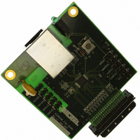
Manufacturer Part Number
KSZ8041NL-EVAL
Description
BOARD EVALUATION FOR KSZ8041NL
Manufacturer
Micrel Inc
Specifications of KSZ8041NL-EVAL
Main Purpose
Interface, Ethernet PHY
Embedded
No
Utilized Ic / Part
KSZ8041NL
Primary Attributes
Single Chip PHY, 10BASE-T/100BASE-TX
Secondary Attributes
MII, RMII, HP Auto MDI, MDI-X Auto Polarity Correction
Lead Free Status / RoHS Status
Lead free / RoHS Compliant
Other names
576-1621


Micrel, Inc.
Pin Description – KSZ8041NL
September 2010
Pin Number
1
2
3
4
5
6
7
8
9
10
11
12
13
14
15
16
17
18
19
Pin Name
GND
VDDPLL_1.8
VDDA_3.3
RX-
RX+
TX-
TX+
XO
XI /
REFCLK
REXT
MDIO
MDC
RXD3 /
PHYAD0
RXD2 /
PHYAD1
RXD1 /
RXD[1] /
PHYAD2
RXD0 /
RXD[0] /
DUPLEX
VDDIO_3.3
RXDV /
CRSDV /
CONFIG2
RXC
Type
Ipu/O
Ipd/O
Ipd/O
Ipu/O
Ipd/O
Gnd
I/O
I/O
I/O
I/O
I/O
I/O
P
P
O
P
O
I
I
(1)
Pin Function
Ground
1.8V analog V
3.3V analog V
Physical receive or transmit signal (- differential)
Physical receive or transmit signal (+ differential)
Physical transmit or receive signal (- differential)
Physical transmit or receive signal (+ differential)
Crystal feedback
This pin is used only in MII mode when a 25 MHz crystal is used.
This pin is a no connect if oscillator or external clock source is used, or if RMII mode
is selected.
Crystal / Oscillator / External Clock Input
MII Mode:
RMII Mode:
Set physical transmit output current
Connect a 6.49KΩ resistor in parallel with a 100pF capacitor to ground on this pin.
See KSZ8041NL reference schematics.
Management Interface (MII) Data I/O
This pin requires an external 4.7KΩ pull-up resistor.
Management Interface (MII) Clock Input
This pin is synchronous to the MDIO data interface.
MII Mode:
Config Mode:
MII Mode:
Config Mode:
MII Mode:
RMII Mode:
Config Mode:
MII Mode:
RMII Mode:
Config Mode:
3.3V digital V
MII Mode:
RMII Mode:
Config Mode:
MII Mode:
DD
DD
DD
The pull-up/pull-down value is latched as PHYADDR[0] during
power-up / reset. See “Strapping Options” section for details.
The pull-up/pull-down value is latched as PHYADDR[1] during
power-up / reset. See “Strapping Options” section for details.
The pull-up/pull-down value is latched as PHYADDR[2] during
power-up / reset. See “Strapping Options” section for details.
Latched as DUPLEX (register 0h, bit 8) during power-up /
reset. See “Strapping Options” section for details.
The pull-up/pull-down value is latched as CONFIG2 during
power-up / reset. See “Strapping Options” section for details.
25MHz +/-50ppm (crystal, oscillator, or external clock)
50MHz +/-50ppm (oscillator, or external clock only)
Receive Data Output[3]
Receive Data Output[2]
Receive Data Output[1]
Receive Data Output[1]
Receive Data Output[0]
Receive Data Output[0]
Receive Data Valid Output /
Carrier Sense/Receive Data Valid Output /
Receive Clock Output
10
(2)
(2)
(2)
(3)
(2)
(3)
/
/
/
/
/
/
M9999-090910-1.4
KSZ8041NL/RNL
Related parts for KSZ8041NL-EVAL
Image
Part Number
Description
Manufacturer
Datasheet
Request
R

Part Number:
Description:
IC TXRX PHY 10/100 LV/LP 32-MLF
Manufacturer:
Micrel Inc
Datasheet:
Part Number:
Description:
Physical Layer Transceiver 10/100BASE-T/TX ( ) - Automotive Qualified
Manufacturer:
Micrel Inc
Datasheet:

Part Number:
Description:
Physical Layer Transceiver 10/100BASE-T/TX ( ) - Automotive Qualified
Manufacturer:
Micrel Inc
Datasheet:

Part Number:
Description:
Manufacturer:
Micrel Inc
Datasheet:
Part Number:
Description:
Manufacturer:
Micrel Inc
Datasheet:
Part Number:
Description:
Manufacturer:
Micrel Inc
Datasheet:
Part Number:
Description:
Manufacturer:
Micrel Inc
Datasheet:
Part Number:
Description:
Manufacturer:
Micrel Inc
Datasheet:
Part Number:
Description:
Manufacturer:
Micrel Inc
Datasheet:
Part Number:
Description:
Manufacturer:
Micrel Inc
Datasheet:
Part Number:
Description:
Manufacturer:
Micrel Inc
Datasheet:
Part Number:
Description:
Manufacturer:
Micrel Inc
Datasheet:
Part Number:
Description:
Manufacturer:
Micrel Inc
Datasheet: