DC-VIDEO-TVP5146N Altera, DC-VIDEO-TVP5146N Datasheet - Page 18
DC-VIDEO-TVP5146N
Manufacturer Part Number
DC-VIDEO-TVP5146N
Description
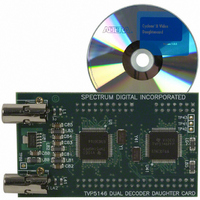
VIDEO DAUGHTER CARD
Manufacturer
Altera
Series
Stratix® IIIr
Datasheets
1.EP3SL150F780C4N.pdf
(16 pages)
2.EP3SL150F780C4N.pdf
(332 pages)
3.DC-VIDEO-TVP5146N.pdf
(58 pages)
Specifications of DC-VIDEO-TVP5146N
Main Purpose
Video, Daughter Card
Embedded
No
Utilized Ic / Part
Altera Dev Kits
Primary Attributes
Dual Composite Video Input - NTSC or PAL
Secondary Attributes
10-bit BT.656 Output, Compatible with Expansion Connector, Standard on Most Altera Development Kits
Lead Free Status / RoHS Status
Lead free / RoHS Compliant
Other names
544-1704


Functional Description
2–10
Stratix II EP2S180 DSP Development Board Reference Manual
The Stratix II EP2S180 DSP development board can obtain a clock source
from one or more of the following sources:
■
■
The board can provide independent clocks from both the enhanced and
fast PLLs to the A/D converters, the D/A converters, and the other
components that require stable clock sources.
To implement this concept, the enhanced PLL5-dedicated pins drive the
A/D converters and associated functions, and the enhanced
PLL6-dedicated pins drive the D/A converters and associated functions.
Notes to
(1)
(2)
pld_CLKIN0,pld_CLK
IN1
pld_CLKIN0_n,pld_C
LKIN1_n
proto1_OSC,
proto2_OSC
cpld_CLKOSC
adc_CLK_IN1,
adc_CLK_IN2
dac_CLKIN1,
dac_CLKIN2
pld_CLKFB
adc_CLK_IN1_n,
adc_CLK_IN2_n
dac_DACCLKIN1,
dac_DACCLKIN2
pld_DACCLKIN
proto1_CLKOUT,
proto2_CLKOUT
Table 2–4. Clock Distribution Signals (Part 2 of 2)
The on-board crystal oscillator
An external clock (through an SMA connector or a Stratix II pin)
Signal Name
J3 and J4 control which clock is routed to the A/D converters. See
details.
J18 and J19 control which clock is routed to the D/A converters. See
for details.
Table
Core Version a.b.c variable
2–4:
100-MHz oscillator
External CLKIN_n input
(J11)
100-MHz oscillator
100-MHz oscillator
100-MHz oscillator
100-MHz oscillator
pld_CLKOUT signal from
the Stratix II pin J14
External CLKIN_n input
(J11)
External DA_EXT_CLK
input (J12)
External DA_EXT_CLK
input (J12)
PROTO1 (J25 pin 13)
PROTO2 (J28 pin 13) via
a buffer (U7)
Comes From
Stratix II device pins AM17
and A16
Stratix II device pins AL17
and B16
PROTO1 (J25 pin 9) and
PROTO2 (J28 pin 9) via a
buffer (U7)
CPLD (U10 pin 125)
ADC A (U1 pins 8, 7) and B
(U2 pins 8, 7)
DAC A (U14 pin 28) and B
(U15 pin 28)
Stratix II device pin U1
ADC A (U1 pins 8, 7) and B
(U2 pins 8, 7)
DAC A (U14 pin 28) and B
(U15 pin 28)
Stratix II device pin E16
Stratix II device pins T32 and
T30
Altera Corporation
Goes To
(2)
(2)
(1)
(1)
Table 2–10
Table 2–16
for
Related parts for DC-VIDEO-TVP5146N
Image
Part Number
Description
Manufacturer
Datasheet
Request
R

Part Number:
Description:
CYCLONE II STARTER KIT EP2C20N
Manufacturer:
Altera
Datasheet:


Part Number:
Description:
CPLD, EP610 Family, ECMOS Process, 300 Gates, 16 Macro Cells, 16 Reg., 16 User I/Os, 5V Supply, 35 Speed Grade, 24DIP
Manufacturer:
Altera Corporation
Datasheet:
Part Number:
Description:
CPLD, EP610 Family, ECMOS Process, 300 Gates, 16 Macro Cells, 16 Reg., 16 User I/Os, 5V Supply, 15 Speed Grade, 24DIP
Manufacturer:
Altera Corporation
Datasheet:
Part Number:
Description:
Manufacturer:
Altera Corporation
Datasheet:
Part Number:
Description:
CPLD, EP610 Family, ECMOS Process, 300 Gates, 16 Macro Cells, 16 Reg., 16 User I/Os, 5V Supply, 30 Speed Grade, 24DIP
Manufacturer:
Altera Corporation
Datasheet:
Part Number:
Description:
High-performance, low-power erasable programmable logic devices with 8 macrocells, 10ns
Manufacturer:
Altera Corporation
Datasheet:
Part Number:
Description:
High-performance, low-power erasable programmable logic devices with 8 macrocells, 7ns
Manufacturer:
Altera Corporation
Datasheet:
Part Number:
Description:
Classic EPLD
Manufacturer:
Altera Corporation
Datasheet:
Part Number:
Description:
High-performance, low-power erasable programmable logic devices with 8 macrocells, 10ns
Manufacturer:
Altera Corporation
Datasheet:
Part Number:
Description:
Manufacturer:
Altera Corporation
Datasheet:
Part Number:
Description:
Manufacturer:
Altera Corporation
Datasheet:
Part Number:
Description:
Manufacturer:
Altera Corporation
Datasheet:
Part Number:
Description:
CPLD, EP610 Family, ECMOS Process, 300 Gates, 16 Macro Cells, 16 Reg., 16 User I/Os, 5V Supply, 25 Speed Grade, 24DIP
Manufacturer:
Altera Corporation
Datasheet: