EVB9303 SMSC, EVB9303 Datasheet - Page 118
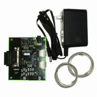
EVB9303
Manufacturer Part Number
EVB9303
Description
EVALUATION BOARD FOR LAN9303
Manufacturer
SMSC
Specifications of EVB9303
Main Purpose
Interface, Ethernet
Embedded
No
Utilized Ic / Part
LAN9303
Primary Attributes
3 Ports, 100BASE-TX/10BASE-T, Managed
Secondary Attributes
Full Duplex and HP Auto-MDIX Support, 10BASE-T and 100BASE-TX
Lead Free Status / Rohs Status
Lead free / RoHS Compliant
Other names
638-1095


Revision 1.4 (07-07-10)
8.5.1
8.5.2
The I
is driven by the master, while the data wire is bi-directional. Both signals are open-drain and require
external pull-up resistors.
The I
speed of 400KHz. Refer to the NXP I
I
The I
A read or write command is started by the master first sending a start condition, followed by a control
byte. The control byte consists of a 7-bit slave address and a 1-bit read/write indication (R/~W). The
slave address used by the device is 0001010b, written as SA6 (first bit on the wire) through SA0 (last
bit on the wire). Assuming the slave address in the control byte matches this address, the control byte
is acknowledged by the device. Otherwise, the entire sequence is ignored until the next start condition.
The I
If the read/write indication (R/~W) in the control byte is a 0 (indicating a potential write), the next byte
sent by the master is the register address. After the address byte is acknowledged by the device, the
master may either send data bytes to be written, or it may send another start condition (to start the
reading of data), or a stop condition. The latter two will terminate the current write (without writing any
data), but will have the affect of setting the internal register address which will be used for subsequent
reads.
If the read/write indication in the control byte is a 1 (indicating a read), the device will start sending
data following the control byte acknowledgement.
Note: All registers are accessed as DWORDs. Appending two 0 bits to the address field will form the
I
Following the device addressing, as detailed in
the master sends a start condition and control byte with the R/~W bit set. Assuming the slave address
in the control byte matches the device address, the control byte is acknowledged by the device.
Otherwise, the entire sequence is ignored until the next start condition. Following the acknowledge,
the device sends 4 bytes of data. The first 3 bytes are acknowledged by the master and on the fourth,
the master sends a no-acknowledge followed by the stop condition. The no-acknowledge informs the
device not to send the next 4 bytes (as it would in the case of a multiple read). The internal register
address is unchanged following the single read.
Multiple reads are performed when the master sends an acknowledge on the fourth byte. The internal
address is incremented and the next register is shifted out. Once the internal address reaches its
maximum, it rolls over to 0. The multiple read is concluded when the master sends a no-acknowledge
followed by a stop condition. The no-acknowledge informs the device not to send the next 4 bytes.
The internal register address in incremented for each read including the final.
2
2
C Slave Command Format
C Slave Read Sequence
2
2
2
2
C slave serial interface consists of a data wire (SDA) and a serial clock (SCL). The serial clock
C slave serial interface supports single register and multiple register read and write commands.
C command format can be seen in
C slave serial interface supports the standard-mode speed of up to 100KHz and the fast-mode
register address. Addresses and data are transferred msb first. Data is transferred MSB first
(little endian).
S
S
A
6
S
A
5
Control Byte
S
A
4
S
A
3
Figure 8.8 I
S
A
2
Small Form Factor Three Port 10/100 Managed Ethernet Switch with Single MII/RMII/Turbo MII
S
A
1
S
A
0
R/~W
DATASHEET
2
0
2
C-Bus Specification for detailed I
C Slave Addressing
A
C
K
118
Figure
A
9
Section
A
8
Address Byte
8.8.
A
7
A
6
8.5.1, a register is read from the device when
A
5
Data [31]
Start or
Stop or
A
4
A
3
A
2
2
A
C
K
C timing information.
*
SMSC LAN9303/LAN9303i
Datasheet
Related parts for EVB9303
Image
Part Number
Description
Manufacturer
Datasheet
Request
R


Part Number:
Description:
FAST ETHERNET PHYSICAL LAYER DEVICE
Manufacturer:
SMSC Corporation
Datasheet:
Part Number:
Description:
357-036-542-201 CARDEDGE 36POS DL .156 BLK LOPRO
Manufacturer:
SMSC Corporation
Datasheet:
Part Number:
Description:
357-036-542-201 CARDEDGE 36POS DL .156 BLK LOPRO
Manufacturer:
SMSC Corporation
Datasheet:
Part Number:
Description:
357-036-542-201 CARDEDGE 36POS DL .156 BLK LOPRO
Manufacturer:
SMSC Corporation
Datasheet:
Part Number:
Description:
4-PORT USB2.0 HUB CONTROLLER
Manufacturer:
SMSC Corporation
Datasheet:
Part Number:
Description:
Manufacturer:
SMSC Corporation
Datasheet:
Part Number:
Description:
Manufacturer:
SMSC Corporation
Datasheet:
Part Number:
Description:
FDC37C672ENHANCED SUPER I/O CONTROLLER WITH FAST IR
Manufacturer:
SMSC Corporation
Datasheet:
Part Number:
Description:
COM90C66LJPARCNET Controller/Transceiver with AT Interface and On-Chip RAM
Manufacturer:
SMSC Corporation
Datasheet:
Part Number:
Description:
Manufacturer:
SMSC Corporation
Datasheet:
Part Number:
Description:
Manufacturer:
SMSC Corporation
Datasheet:
Part Number:
Description:
Manufacturer:
SMSC Corporation
Datasheet:
Part Number:
Description:
Manufacturer:
SMSC Corporation
Datasheet: