AD9520-1/PCBZ Analog Devices Inc, AD9520-1/PCBZ Datasheet - Page 2
AD9520-1/PCBZ
Manufacturer Part Number
AD9520-1/PCBZ
Description
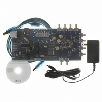
BOARD EVAL FOR AD9520-1
Manufacturer
Analog Devices Inc
Specifications of AD9520-1/PCBZ
Design Resources
Synchronizing Multiple AD9910 1 GSPS Direct Digital Synthesizers (CN0121) Phase Coherent FSK Modulator (CN0186)
Main Purpose
Timing, Clock Generator
Embedded
No
Utilized Ic / Part
AD9520-1
Primary Attributes
12 LVPECL/24 CMOS Output Clock Generator with 2.5 GHz VCO
Secondary Attributes
SPI and I2C Compatible Control Port
Silicon Manufacturer
Analog Devices
Application Sub Type
PLL Clock Synthesizer
Kit Application Type
Clock & Timing
Silicon Core Number
AD9520-0, AD9520-2, AD9520-2
Silicon Family Name
AD9520-X
Rohs Compliant
Yes
Lead Free Status / RoHS Status
Lead free / RoHS Compliant


AD9520-1
TABLE OF CONTENTS
Features .............................................................................................. 1
Applications ....................................................................................... 1
General Description ......................................................................... 1
Functional Block Diagram .............................................................. 1
Revision History ............................................................................... 3
Specifications ..................................................................................... 4
Absolute Maximum Ratings .......................................................... 17
Pin Configuration and Function Descriptions ........................... 18
Typical Performance Characteristics ........................................... 21
Terminology .................................................................................... 26
Detailed Block Diagram ................................................................ 27
Power Supply Requirements ....................................................... 4
PLL Characteristics ...................................................................... 4
Clock Inputs .................................................................................. 7
Clock Outputs ............................................................................... 7
Timing Characteristics ................................................................ 8
Clock Output Additive Phase Noise (Distribution Only;
VCO Divider Not Used) ............................................................ 10
Clock Output Absolute Phase Noise (Internal VCO Used) .. 11
Clock Output Absolute Time Jitter (Clock Generation
Using Internal VCO) .................................................................. 11
Clock Output Absolute Time Jitter (Clock Cleanup
Using Internal VCO) .................................................................. 11
Clock Output Absolute Time Jitter (Clock Generation
Using External VCXO) .............................................................. 12
Clock Output Additive Time Jitter
(VCO Divider Not Used) .......................................................... 12
Clock Output Additive Time Jitter (VCO Divider Used) ..... 13
Serial Control Port—SPI Mode ................................................ 13
Serial Control Port—I2C Mode ................................................ 14
PD , SYNC , and RESET Pins ..................................................... 15
Serial Port Setup Pins: SP1, SP0 ............................................... 15
LD, STATUS, and REFMON Pins ............................................ 15
Power Dissipation ....................................................................... 16
Thermal Resistance .................................................................... 17
ESD Caution ................................................................................ 17
Timing Diagrams ..................................................................... 9
Rev. 0 | Page 2 of 84
Theory of Operation ...................................................................... 28
Operational Configurations ...................................................... 28
Zero Delay Operation ................................................................ 43
Clock Distribution ..................................................................... 44
Mode 0: Internal VCO and Clock Distribution ................. 28
Mode 1: Clock Distribution or External
VCO < 1600 MHz .................................................................. 30
Mode 2: High Frequency Clock Distribution—CLK or
External VCO > 1600 MHz .................................................. 32
Phase-Locked Loop (PLL) .................................................... 34
Configuration of the PLL ...................................................... 34
Phase Frequency Detector (PFD) ........................................ 34
Charge Pump (CP) ................................................................. 35
On-Chip VCO ........................................................................ 35
PLL External Loop Filter ....................................................... 35
PLL Reference Inputs ............................................................. 35
Reference Switchover ............................................................. 36
Reference Divider R ............................................................... 36
VCO/VCXO Feedback Divider N: P, A, B, R ..................... 36
Digital Lock Detect (DLD) ................................................... 38
Analog Lock Detect (ALD) ................................................... 38
Current Source Digital Lock Detect (CSDLD) .................. 38
External VCXO/VCO Clock Input (CLK/ CLK ) ................ 39
Holdover .................................................................................. 39
External/Manual Holdover Mode ........................................ 39
Automatic/Internal Holdover Mode .................................... 39
Frequency Status Monitors ................................................... 41
VCO Calibration .................................................................... 42
Internal Zero Delay Mode ..................................................... 43
External Zero Delay Mode .................................................... 43
Operation Modes ................................................................... 44
CLK or VCO Direct-to-LVPECL Outputs .......................... 44
Clock Frequency Division ..................................................... 45
VCO Divider ........................................................................... 45
Channel Dividers ................................................................... 45
Synchronizing the Outputs— SYNC Function ................... 47
LVPECL Output Drivers ....................................................... 49
CMOS Output Drivers .......................................................... 49
Related parts for AD9520-1/PCBZ
Image
Part Number
Description
Manufacturer
Datasheet
Request
R

Part Number:
Description:
12/24 Channel Clock Gen 2,0GH
Manufacturer:
Analog Devices Inc
Datasheet:

Part Number:
Description:
12/24 Channel Clock Gen 2,0GH
Manufacturer:
Analog Devices Inc
Datasheet:
Part Number:
Description:
12/24 Channel Clock Gen 2,0GH
Manufacturer:
Analog Devices Inc
Datasheet:
Part Number:
Description:
12/24 Channel Clock Gen 2,0GH
Manufacturer:
Analog Devices Inc
Datasheet:
Part Number:
Description:
12/24 Channel Clock Gen 2,0GH
Manufacturer:
Analog Devices Inc
Datasheet:
Part Number:
Description:
Clock IC With 2.8GHz On-chip VCO
Manufacturer:
Analog Devices Inc
Datasheet:
Part Number:
Description:
Lock IC With 2.8GHz On-chip VCO
Manufacturer:
Analog Devices Inc
Datasheet:
Part Number:
Description:
12/24 Channel Clock Gen 2,5 GHz VCO
Manufacturer:
Analog Devices Inc
Datasheet:
Part Number:
Description:
12/24 Channel Clock Distribution W/ On-C
Manufacturer:
Analog Devices Inc
Datasheet:
Part Number:
Description:
12/24 Channel Clock Gen 2,25GH
Manufacturer:
Analog Devices Inc
Datasheet:
Part Number:
Description:
12/24 Channel Clock Distribution W/ On-C
Manufacturer:
Analog Devices Inc
Datasheet:
Part Number:
Description:
12/24 Channel Clock Distribution W/ On-C
Manufacturer:
Analog Devices Inc
Datasheet:
Part Number:
Description:
Clock IC With 1.6GHz On-chip VCO
Manufacturer:
Analog Devices Inc
Datasheet:
Part Number:
Description:
Clock IC With 1.6GHz On-chip VCO
Manufacturer:
Analog Devices Inc
Datasheet:
Part Number:
Description:
12/24-Output Clock Generator
Manufacturer:
Analog Devices Inc
Datasheet: