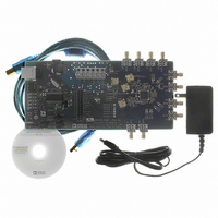
AD9520-1/PCBZ Analog Devices Inc, AD9520-1/PCBZ Datasheet - Page 33

AD9520-1/PCBZ
Manufacturer Part Number
AD9520-1/PCBZ
Description
BOARD EVAL FOR AD9520-1
Manufacturer
Analog Devices Inc
Specifications of AD9520-1/PCBZ
Design Resources
Synchronizing Multiple AD9910 1 GSPS Direct Digital Synthesizers (CN0121) Phase Coherent FSK Modulator (CN0186)
Main Purpose
Timing, Clock Generator
Embedded
No
Utilized Ic / Part
AD9520-1
Primary Attributes
12 LVPECL/24 CMOS Output Clock Generator with 2.5 GHz VCO
Secondary Attributes
SPI and I2C Compatible Control Port
Silicon Manufacturer
Analog Devices
Application Sub Type
PLL Clock Synthesizer
Kit Application Type
Clock & Timing
Silicon Core Number
AD9520-0, AD9520-2, AD9520-2
Silicon Family Name
AD9520-X
Rohs Compliant
Yes
Lead Free Status / RoHS Status
Lead free / RoHS Compliant
- Current page: 33 of 84
- Download datasheet (2Mb)
OPTIONAL
SCLK/SCL
SDIO/SDA
EEPROM
BYPASS
RESET
REFIN
REFIN
SYNC
SDO
CLK
CLK
SP1
SP0
PD
CS
LF
REF1
REF2
REGULATOR (LDO)
DECODE
SERIAL
PORT
LOW DROPOUT
DIGITAL
LOGIC
INTERFACE
AMP
BUF
SPI
SWITCHOVER
STATUS
REFERENCE
REF_SEL
AD9520
EEPROM
STATUS
INTERFACE
Figure 39. High Frequency Clock Distribution or External VCO > 1600 MHz (Mode 2)
I
2
C
VS
PRESCALER
ZERO DELAY BLOCK
2, 3, 4, 5, OR 6
DIVIDE BY 1,
1
P, P + 1
GND
0
N DIVIDER
STATUS
COUNTERS
DISTRIBUTION
REFERENCE
A/B
RSET
Rev. 0 | Page 33 of 84
DIVIDE BY
DIVIDE BY
DIVIDE BY
DIVIDE BY
1 TO 32
1 TO 32
1 TO 32
1 TO 32
PROGRAMMABLE
REFMON
N DELAY
FREQUENCY
DETECTOR
DETECT
PHASE
LOCK
CPRSET VCP
CHARGE
PUMP
HOLD
AD9520-1
OUT0
OUT0
OUT1
OUT1
OUT2
OUT2
OUT3
OUT3
OUT4
OUT4
OUT5
OUT5
OUT6
OUT6
OUT7
OUT7
OUT8
OUT8
OUT9
OUT9
OUT10
OUT10
OUT11
OUT11
LD
CP
STATUS
VS_DRV
Related parts for AD9520-1/PCBZ
Image
Part Number
Description
Manufacturer
Datasheet
Request
R

Part Number:
Description:
12/24 Channel Clock Gen 2,0GH
Manufacturer:
Analog Devices Inc
Datasheet:

Part Number:
Description:
12/24 Channel Clock Gen 2,0GH
Manufacturer:
Analog Devices Inc
Datasheet:

Part Number:
Description:
12/24 Channel Clock Gen 2,0GH
Manufacturer:
Analog Devices Inc
Datasheet:

Part Number:
Description:
12/24 Channel Clock Gen 2,0GH
Manufacturer:
Analog Devices Inc
Datasheet:

Part Number:
Description:
12/24 Channel Clock Gen 2,0GH
Manufacturer:
Analog Devices Inc
Datasheet:

Part Number:
Description:
Clock IC With 2.8GHz On-chip VCO
Manufacturer:
Analog Devices Inc
Datasheet:

Part Number:
Description:
Lock IC With 2.8GHz On-chip VCO
Manufacturer:
Analog Devices Inc
Datasheet:

Part Number:
Description:
12/24 Channel Clock Gen 2,5 GHz VCO
Manufacturer:
Analog Devices Inc
Datasheet:

Part Number:
Description:
12/24 Channel Clock Distribution W/ On-C
Manufacturer:
Analog Devices Inc
Datasheet:

Part Number:
Description:
12/24 Channel Clock Gen 2,25GH
Manufacturer:
Analog Devices Inc
Datasheet:

Part Number:
Description:
12/24 Channel Clock Distribution W/ On-C
Manufacturer:
Analog Devices Inc
Datasheet:

Part Number:
Description:
12/24 Channel Clock Distribution W/ On-C
Manufacturer:
Analog Devices Inc
Datasheet:

Part Number:
Description:
Clock IC With 1.6GHz On-chip VCO
Manufacturer:
Analog Devices Inc
Datasheet:

Part Number:
Description:
Clock IC With 1.6GHz On-chip VCO
Manufacturer:
Analog Devices Inc
Datasheet:

Part Number:
Description:
12/24-Output Clock Generator
Manufacturer:
Analog Devices Inc
Datasheet:


