AD9520-1/PCBZ Analog Devices Inc, AD9520-1/PCBZ Datasheet - Page 53
AD9520-1/PCBZ
Manufacturer Part Number
AD9520-1/PCBZ
Description
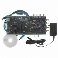
BOARD EVAL FOR AD9520-1
Manufacturer
Analog Devices Inc
Specifications of AD9520-1/PCBZ
Design Resources
Synchronizing Multiple AD9910 1 GSPS Direct Digital Synthesizers (CN0121) Phase Coherent FSK Modulator (CN0186)
Main Purpose
Timing, Clock Generator
Embedded
No
Utilized Ic / Part
AD9520-1
Primary Attributes
12 LVPECL/24 CMOS Output Clock Generator with 2.5 GHz VCO
Secondary Attributes
SPI and I2C Compatible Control Port
Silicon Manufacturer
Analog Devices
Application Sub Type
PLL Clock Synthesizer
Kit Application Type
Clock & Timing
Silicon Core Number
AD9520-0, AD9520-2, AD9520-2
Silicon Family Name
AD9520-X
Rohs Compliant
Yes
Lead Free Status / RoHS Status
Lead free / RoHS Compliant


Data Transfer Format
Send byte format—the send byte protocol is used to set up the register address for subsequent commands.
S
Write byte format—the write byte protocol is used to write a register address to the RAM starting from the specified RAM address.
S
Receive byte format—the receive byte protocol is used to read the data byte(s) from RAM starting from the current address.
S
Read byte format—the combined format of the send byte and the receive byte.
S
I²C Serial Port Timing
Table 42. I2C Timing Definitions
Parameter
f
t
t
t
t
t
t
t
t
t
t
t
I2C
IDLE
HLD; STR
SET; STR
SET; STP
HLD; DAT
SET; DAT
LOW
HIGH
RISE
FALL
SPIKE
Slave Address
Slave
Address
SDA
SCL
Slave Address
Slave Address
t
FALL
S
W
A
t
W
HLD; STR
t
LOW
RAM Address
High Byte
A
Description
I²C clock frequency
Bus idle time between stop and start conditions
Hold time for repeated start condition
Setup time for repeated start condition
Setup time for stop condition
Hold time for data
Setup time for data
Duration of SCL clock low
Duration of SCL clock high
SCL/SDA rise time
SCL/SDA fall time
Voltage spike pulse width that must be suppressed by the input filter
W
RAM Address
High Byte
R
t
t
RISE
SET; DAT
t
HLD; DAT
A
A
A
RAM Address High Byte
RAM Data 0
RAM Address
Low Byte
t
HIGH
A
RAM Address
Low Byte
t
FALL
Figure 60. I²C Serial Port Timing
Rev. 0 | Page 53 of 84
t
SET; STR
A
A
Sr
A
Slave
Address
Sr
RAM Data 1
RAM Data 0
t
HLD; STR
A
R
A
RAM Address Low Byte
A
RAM
Data 0
RAM Data 1
t
SPIKE
A
t
SET; STP
A
RAM Data 2
t
RISE
RAM
Data 1
P
A
t
IDLE
RAM Data 2
A
RAM
Data 2
AD9520-1
S
A
A
A
A
P
P
P
P
Related parts for AD9520-1/PCBZ
Image
Part Number
Description
Manufacturer
Datasheet
Request
R

Part Number:
Description:
12/24 Channel Clock Gen 2,0GH
Manufacturer:
Analog Devices Inc
Datasheet:

Part Number:
Description:
12/24 Channel Clock Gen 2,0GH
Manufacturer:
Analog Devices Inc
Datasheet:
Part Number:
Description:
12/24 Channel Clock Gen 2,0GH
Manufacturer:
Analog Devices Inc
Datasheet:
Part Number:
Description:
12/24 Channel Clock Gen 2,0GH
Manufacturer:
Analog Devices Inc
Datasheet:
Part Number:
Description:
12/24 Channel Clock Gen 2,0GH
Manufacturer:
Analog Devices Inc
Datasheet:
Part Number:
Description:
Clock IC With 2.8GHz On-chip VCO
Manufacturer:
Analog Devices Inc
Datasheet:
Part Number:
Description:
Lock IC With 2.8GHz On-chip VCO
Manufacturer:
Analog Devices Inc
Datasheet:
Part Number:
Description:
12/24 Channel Clock Gen 2,5 GHz VCO
Manufacturer:
Analog Devices Inc
Datasheet:
Part Number:
Description:
12/24 Channel Clock Distribution W/ On-C
Manufacturer:
Analog Devices Inc
Datasheet:
Part Number:
Description:
12/24 Channel Clock Gen 2,25GH
Manufacturer:
Analog Devices Inc
Datasheet:
Part Number:
Description:
12/24 Channel Clock Distribution W/ On-C
Manufacturer:
Analog Devices Inc
Datasheet:
Part Number:
Description:
12/24 Channel Clock Distribution W/ On-C
Manufacturer:
Analog Devices Inc
Datasheet:
Part Number:
Description:
Clock IC With 1.6GHz On-chip VCO
Manufacturer:
Analog Devices Inc
Datasheet:
Part Number:
Description:
Clock IC With 1.6GHz On-chip VCO
Manufacturer:
Analog Devices Inc
Datasheet:
Part Number:
Description:
12/24-Output Clock Generator
Manufacturer:
Analog Devices Inc
Datasheet: