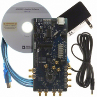
AD9520-4/PCBZ Analog Devices Inc, AD9520-4/PCBZ Datasheet - Page 20

AD9520-4/PCBZ
Manufacturer Part Number
AD9520-4/PCBZ
Description
BOARD EVAL FOR AD9520-4
Manufacturer
Analog Devices Inc
Specifications of AD9520-4/PCBZ
Design Resources
Synchronizing Multiple AD9910 1 GSPS Direct Digital Synthesizers (CN0121) Phase Coherent FSK Modulator (CN0186)
Main Purpose
Timing, Clock Generator
Embedded
No
Utilized Ic / Part
AD9520-4
Primary Attributes
1.4 ~ 1.8 GHz Output Frequency
Secondary Attributes
Accepts CMOS, LVDS, or LVPECL References Up to 250 MHz
Silicon Manufacturer
Analog Devices
Application Sub Type
PLL Clock Synthesizer
Kit Application Type
Clock & Timing
Silicon Core Number
AD9520-0, AD9520-2, AD9520-2
Silicon Family Name
AD9520-X
Rohs Compliant
Yes
Lead Free Status / RoHS Status
Lead free / RoHS Compliant
AD9520-4
Pin No.
47
48
50
51
52
53
55
56
58
62
63
64
EPAD
Input/
Output
O
O
O
O
O
O
O
O
O
O
I
I
Pin
Type
LVPECL or
CMOS
LVPECL or
CMOS
LVPECL or
CMOS
LVPECL or
CMOS
LVPECL or
CMOS
LVPECL or
CMOS
LVPECL or
CMOS
LVPECL or
CMOS
Current set
resistor
Current set
resistor
Reference
input
Reference
input
GND
Mnemonic
OUT3 (OUT3B)
OUT3 (OUT3A)
OUT2 (OUT2B)
OUT2 (OUT2A)
OUT1 (OUT1B)
OUT1 (OUT1A)
OUT0 (OUT0B)
OUT0 (OUT0A)
RSET
CPRSET
REFIN (REF2)
REFIN (REF1)
GND
output, or as a single-ended CMOS output.
Clock Output. This pin can be configured as one side of a differential LVPECL
output, or as a single-ended CMOS output.
output, or as a single-ended CMOS output.
Clock Output. This pin can be configured as one side of a differential LVPECL
output, or as a single-ended CMOS output.
output, or as a single-ended CMOS output.
Clock Output. This pin can be configured as one side of a differential LVPECL
output, or as a single-ended CMOS output.
output, or as a single-ended CMOS output.
Clock Output. This pin can be configured as one side of a differential LVPECL
output, or as a single-ended CMOS output.
Clock Distribution Current Set Resistor. Connect a 4.12 kΩ resistor from this
pin to GND.
Charge Pump Current Set Resistor. Connect a 5.1 kΩ resistor from this pin to GND.
Along with REFIN, this is the differential input for the PLL reference. Alternatively,
this pin is a single-ended input for REF2.
Along with REFIN, this is the differential input for the PLL reference. Alternatively,
this pin is a single-ended input for REF1.
Exposed die pad must be connected to GND.
Description
Clock Output. This pin can be configured as one side of a differential LVPECL
Clock Output. This pin can be configured as one side of a differential LVPECL
Clock Output. This pin can be configured as one side of a differential LVPECL
Clock Output. This pin can be configured as one side of a differential LVPECL
Rev. 0 | Page 20 of 84


