CDB5376 Cirrus Logic Inc, CDB5376 Datasheet - Page 68
CDB5376
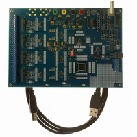
Manufacturer Part Number
CDB5376
Description
EVALUATION BOARD FOR CS5376
Manufacturer
Cirrus Logic Inc
Datasheets
1.CS5371A-ISZR.pdf
(32 pages)
2.CS4373A-ISZ.pdf
(34 pages)
3.CS5376A-IQZR.pdf
(106 pages)
4.CDB5378.pdf
(16 pages)
5.CDB5376.pdf
(80 pages)
6.CDB5376.pdf
(16 pages)
Specifications of CDB5376
Main Purpose
Seismic Evaluation System
Embedded
Yes, MCU, 8-Bit
Utilized Ic / Part
CS3301A, CS3302A, CS4373A, CS5372A, CS5376A
Primary Attributes
Quad Digital Filter
Secondary Attributes
Graphical User Interface, SPI™ & USB Interfaces
Processor To Be Evaluated
CS330x, CS4373A, CS537x
Interface Type
USB
Lead Free Status / RoHS Status
Contains lead / RoHS non-compliant
Lead Free Status / RoHS Status
Lead free / RoHS Compliant, Contains lead / RoHS non-compliant
Other names
598-1778


19.GENERAL PURPOSE I/O
The General Purpose I/O (GPIO) block provides 12
general purpose pins to interface with external
hardware.
19.1 Pin Descriptions
GPIO[4:0]:CS[4:0] - Pins 32 - 36
Standard GPIO pins also used as SPI 2 chip selects.
GPIO[5:10] - Pins 37, 41 - 45
Standard GPIO pins.
GPIO11:EECS - Pin 46
Standard GPIO pin also used as an SPI 1 chip select
when booting from an external EEPROM.
19.2 GPIO Architecture
Each GPIO pin can be configured as input or out-
put, high or low, with a weak (~200 kΩ) internal
pull-up resistor enabled or disabled. Several GPIO
pins also double as chip selects for the SPI 1 and
SPI 2 serial ports. Figure 36 shows the structure of
a bi-directional GPIO pin with SPI chip select func-
tionality.
When the CS5376A is used as an SPI master, either
when booting from EEPROM using SPI 1 or per-
forming master mode transactions using SPI 2, the
chip select signals from SPI 1 and SPI 2 are logi-
cally AND-ed with the GPIO data bit. The corre-
68
CS output from SPI
Data bit
Figure 36. GPIO Bi-directional Structure
GP_PULL
GP_DATA
GP_DIR
sponding GPIO pin should be initialized as output
mode and logical 1 to produce the chip select fall-
ing edge.
19.3 GPIO Registers
When used as standard GPIO pins, settings are pro-
grammed in the GPCFG0 and GPCFG1 registers.
GP_DIR bits set the input/output mode, GP_PULL
bits enable/disable the internal pull-up resistor, and
GP_DATA bits set the output data value. After re-
set, GPIO pins default as inputs with pull-up resis-
tors enabled.
19.4 GPIO Input Mode
When reading a value from the GP_DATA bits, the
returned data reports the current state of the pins. If
a pin is externally driven high it reads a logical 1, if
externally driven low it reads a logical 0. When a
GPIO pin is used as an input, the pull-up resistor
should be disabled to save power if it isn’t required.
19.5 GPIO Output Mode
When a GPIO pin is programmed as an output with
a data value of 0, the pin is driven low and the in-
ternal pull-up resistor is automatically disabled.
When programmed as an output with a data value
of 1, the pin is driven high and the pull-up resistor
is inconsequential.
Pull Up
Logic
R
GPIO/CS
CS5376A
DS612F4
Related parts for CDB5376
Image
Part Number
Description
Manufacturer
Datasheet
Request
R

Part Number:
Description:
Development Kit
Manufacturer:
Cirrus Logic Inc
Datasheet:
Part Number:
Description:
Development Kit
Manufacturer:
Cirrus Logic Inc
Datasheet:


Part Number:
Description:
High-efficiency PFC + Fluorescent Lamp Driver Reference Design
Manufacturer:
Cirrus Logic Inc
Datasheet:
Part Number:
Description:
Development Kit
Manufacturer:
Cirrus Logic Inc
Datasheet:
Part Number:
Description:
Development Kit
Manufacturer:
Cirrus Logic Inc
Datasheet:

Part Number:
Description:
Development Kit
Manufacturer:
Cirrus Logic Inc
Datasheet:
Part Number:
Description:
Development Kit
Manufacturer:
Cirrus Logic Inc
Datasheet:
Part Number:
Description:
Development Kit
Manufacturer:
Cirrus Logic Inc
Datasheet:
Part Number:
Description:
Development Kit
Manufacturer:
Cirrus Logic Inc
Datasheet:

Part Number:
Description:
EVALUATION BOARD FOR CS8427
Manufacturer:
Cirrus Logic Inc
Datasheet:

Part Number:
Description:
BOARD EVAL FOR CS8416 RCVR
Manufacturer:
Cirrus Logic Inc
Datasheet:

Part Number:
Description:
EVALUATION BOARD FOR CS8420
Manufacturer:
Cirrus Logic Inc
Datasheet:

Part Number:
Description:
KIT DEVELOPMENT EP9315 ARM9
Manufacturer:
Cirrus Logic Inc
Datasheet:

Part Number:
Description:
KIT DEVELOPMENT EP9302 ARM9
Manufacturer:
Cirrus Logic Inc
Datasheet: