CDB5345 Cirrus Logic Inc, CDB5345 Datasheet - Page 27
CDB5345
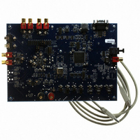
Manufacturer Part Number
CDB5345
Description
EVALUATION BOARD FOR CS5345
Manufacturer
Cirrus Logic Inc
Specifications of CDB5345
Number Of Adc's
2
Number Of Bits
24
Sampling Rate (per Second)
192k
Data Interface
Serial
Inputs Per Adc
6 Single Ended
Power (typ) @ Conditions
400mW @ 5 V
Voltage Supply Source
Analog and Digital
Operating Temperature
-10°C ~ 70°C
Utilized Ic / Part
CS5345
Description/function
Audio A/D
Operating Supply Voltage
5 V
Product
Audio Modules
For Use With/related Products
CS5345
Lead Free Status / RoHS Status
Contains lead / RoHS non-compliant
Lead Free Status / RoHS Status
Lead free / RoHS Compliant, Contains lead / RoHS non-compliant
Other names
598-1780


DS658F2
SCL
SDA
SDA
SCL
START
START
be connected through a resistor to VLC or DGND as desired. The state of the pins is sensed while the
CS5345 is being reset.
The signal timings for a read and write cycle are shown in
defined as a falling transition of SDA while the clock is high. A Stop condition is a rising transition while
the clock is high. All other transitions of SDA occur while the clock is low. The first byte sent to the CS5345
after a Start condition consists of a 7-bit chip address field and a R/W bit (high for a read, low for a write).
The upper 5 bits of the 7-bit address field are fixed at 10011. To communicate with a CS5345, the chip
address field, which is the first byte sent to the CS5345, should match 10011 followed by the settings of
the AD1 and AD0. The eighth bit of the address is the R/W bit. If the operation is a write, the next byte is
the Memory Address Pointer (MAP) which selects the register to be read or written. If the operation is a
read, the contents of the register pointed to by the MAP will be output. Following each data byte, the mem-
ory address pointer will automatically increment to facilitate block reads and writes of successive regis-
ters. Each byte is separated by an acknowledge bit. The ACK bit is output from the CS5345 after each
input byte is read, and is input to the CS5345 from the microcontroller after each transmitted byte.
Since the read operation cannot set the MAP, an aborted write operation is used as a preamble. As shown
in
dition. The following pseudocode illustrates an aborted write operation followed by a read operation.
Send start condition.
Send 10011xx0 (chip address & write operation).
Receive acknowledge bit.
Send MAP byte.
Receive acknowledge bit.
Send stop condition, aborting write.
Send start condition.
Send 10011xx1(chip address & read operation).
Receive acknowledge bit.
0
1
Figure
CHIP ADDRESS (WRITE)
0
1
1
0
CHIP ADDRESS (WRITE)
0
1
2
0
1
3
12, the write operation is aborted after the acknowledge for the MAP byte by sending a stop con-
2
0
1 AD1 AD0 0
4
1
3
5
1 AD1 AD0 0
4
6
5
7
ACK
6
8
7
9
7
ACK
10 11
8
Figure 11. Control Port Timing, I²C Write
6
Figure 12. Control Port Timing, I²C Read
9
6
5
MAP BYTE
12 13 14 15
10 11
6
4
3
MAP BYTE
5
12
2
4
1
13 14 15
3
16
0
ACK
2
STOP
17 18
START
1
16 17 18
0
19
ACK
1
20 21 22 23 24
CHIP ADDRESS (READ)
0
7
0
19
1
6
DATA
Figure 11
1 AD1 AD0 1
24 25
1
0
25
ACK
26
26 27 28
and
ACK
27 28
7
7
DATA +1
DATA
6
Figure
0
1
ACK
0
12. A Start condition is
DATA +1
7
7
0
DATA +n
6
DATA + n
7
1
0
CS5345
0
ACK
ACK
NO
STOP
STOP
27
Related parts for CDB5345
Image
Part Number
Description
Manufacturer
Datasheet
Request
R

Part Number:
Description:
Development Kit
Manufacturer:
Cirrus Logic Inc
Datasheet:
Part Number:
Description:
Development Kit
Manufacturer:
Cirrus Logic Inc
Datasheet:


Part Number:
Description:
High-efficiency PFC + Fluorescent Lamp Driver Reference Design
Manufacturer:
Cirrus Logic Inc
Datasheet:
Part Number:
Description:
Development Kit
Manufacturer:
Cirrus Logic Inc
Datasheet:
Part Number:
Description:
Development Kit
Manufacturer:
Cirrus Logic Inc
Datasheet:

Part Number:
Description:
Development Kit
Manufacturer:
Cirrus Logic Inc
Datasheet:
Part Number:
Description:
Development Kit
Manufacturer:
Cirrus Logic Inc
Datasheet:
Part Number:
Description:
Development Kit
Manufacturer:
Cirrus Logic Inc
Datasheet:
Part Number:
Description:
Development Kit
Manufacturer:
Cirrus Logic Inc
Datasheet:

Part Number:
Description:
EVALUATION BOARD FOR CS8427
Manufacturer:
Cirrus Logic Inc
Datasheet:

Part Number:
Description:
BOARD EVAL FOR CS8416 RCVR
Manufacturer:
Cirrus Logic Inc
Datasheet:

Part Number:
Description:
EVALUATION BOARD FOR CS8420
Manufacturer:
Cirrus Logic Inc
Datasheet:

Part Number:
Description:
KIT DEVELOPMENT EP9315 ARM9
Manufacturer:
Cirrus Logic Inc
Datasheet:

Part Number:
Description:
KIT DEVELOPMENT EP9302 ARM9
Manufacturer:
Cirrus Logic Inc
Datasheet: