CDB5529 Cirrus Logic Inc, CDB5529 Datasheet - Page 11
CDB5529
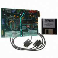
Manufacturer Part Number
CDB5529
Description
EVAL BOARD FOR CS5529
Manufacturer
Cirrus Logic Inc
Specifications of CDB5529
Number Of Adc's
1
Number Of Bits
16
Sampling Rate (per Second)
303
Data Interface
Serial
Inputs Per Adc
2 Differential
Input Range
±2.5 V
Power (typ) @ Conditions
2.6mW @ 2.5 V
Voltage Supply Source
Analog and Digital, Dual ±
Operating Temperature
-40°C ~ 85°C
Utilized Ic / Part
CS5529
Lead Free Status / RoHS Status
Contains lead / RoHS non-compliant
Other names
598-1015


ages. The differential voltage between VREF+ and
VREF- sets the nominal full scale input span of the
converter. For a single-ended reference voltage,
such as the LT1019-2.5, the reference output is
connected to the VREF+ pin of the CS5529 and the
ground reference for the LT1019-2.5 is connected
to the VREF- pin.
Serial Port
The CS5529 includes a microcontroller with a
command register, a configuration register, a con-
version data register (read only), and a gain and off-
set register for calibration. All registers, except the
8-bit command register, are 24-bits in length. Fig-
DS246F5
V ≤ 25mV
i = fV C
n
os
Figure 1. Input models for AIN+ and AIN- pins.
AIN
os
Offset Register (1 × 24)
f = 32.768 kHz
φ Coarse
1
φ Fine
C = 20pF
1
Latch Outputs
Low Power Mode
Output Word Rates
Unipolar/Bipolar
Reset System
etc.
Configuration Register (1 × 24)
Gain Register (1 × 24)
Figure 3. CS5529 Register Diagram.
ure 3 illustrates a block diagram of all the internal
register.
After a system initialization or reset, the serial port
is set to the command mode. The converter stays in
this mode until a valid 8-bit command is received
(the first 8-bits into the serial port). Once a valid 8-
bit command is received and interpreted by the
ADC’s command register, the serial port enters the
data mode. In data mode the next 24 serial clock
pulses shift data either into or out of the serial port
(72 serial clock pulses are needed if the setup reg-
ister command is issued). The Command Register
Descriptions section illustrates all valid com-
mands.
V ≤ 25mV
i = fV C
n
Figure 2. Input model for VREF+ and VREF- pins.
os
VREF
os
Command Register (1 × 8)
f = 32.768 kHz
Conversion Data Register (1x24)
Interface
Serial
φ Coarse
2
φ Fine
C = 10pF
1
CS5529
CS
SDI
SDO
SCLK
11
Related parts for CDB5529
Image
Part Number
Description
Manufacturer
Datasheet
Request
R

Part Number:
Description:
Development Kit
Manufacturer:
Cirrus Logic Inc
Datasheet:
Part Number:
Description:
Development Kit
Manufacturer:
Cirrus Logic Inc
Datasheet:


Part Number:
Description:
High-efficiency PFC + Fluorescent Lamp Driver Reference Design
Manufacturer:
Cirrus Logic Inc
Datasheet:
Part Number:
Description:
Development Kit
Manufacturer:
Cirrus Logic Inc
Datasheet:
Part Number:
Description:
Development Kit
Manufacturer:
Cirrus Logic Inc
Datasheet:

Part Number:
Description:
Development Kit
Manufacturer:
Cirrus Logic Inc
Datasheet:
Part Number:
Description:
Development Kit
Manufacturer:
Cirrus Logic Inc
Datasheet:
Part Number:
Description:
Development Kit
Manufacturer:
Cirrus Logic Inc
Datasheet:
Part Number:
Description:
Development Kit
Manufacturer:
Cirrus Logic Inc
Datasheet:

Part Number:
Description:
EVALUATION BOARD FOR CS8427
Manufacturer:
Cirrus Logic Inc
Datasheet:

Part Number:
Description:
BOARD EVAL FOR CS8416 RCVR
Manufacturer:
Cirrus Logic Inc
Datasheet:

Part Number:
Description:
EVALUATION BOARD FOR CS8420
Manufacturer:
Cirrus Logic Inc
Datasheet:

Part Number:
Description:
KIT DEVELOPMENT EP9315 ARM9
Manufacturer:
Cirrus Logic Inc
Datasheet:

Part Number:
Description:
KIT DEVELOPMENT EP9302 ARM9
Manufacturer:
Cirrus Logic Inc
Datasheet: