CDB5529 Cirrus Logic Inc, CDB5529 Datasheet - Page 18
CDB5529
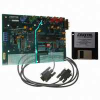
Manufacturer Part Number
CDB5529
Description
EVAL BOARD FOR CS5529
Manufacturer
Cirrus Logic Inc
Specifications of CDB5529
Number Of Adc's
1
Number Of Bits
16
Sampling Rate (per Second)
303
Data Interface
Serial
Inputs Per Adc
2 Differential
Input Range
±2.5 V
Power (typ) @ Conditions
2.6mW @ 2.5 V
Voltage Supply Source
Analog and Digital, Dual ±
Operating Temperature
-40°C ~ 85°C
Utilized Ic / Part
CS5529
Lead Free Status / RoHS Status
Contains lead / RoHS non-compliant
Other names
598-1015


Gain Register
The gain register span is from 0 to (4-2
The gain calibration results is stored in the gain
register. The result sets the slope of the ADC’s
transfer function. The gain register spans from 0 to
(4 - 2
gain register is
where the binary numbers have a value of either
zero or one (b
Self Calibration
The CS5529 offers both self offset and self gain
calibrations. For the self-calibration of offset, the
converter internally ties the inputs of the modulator
together and routes them to the VREF- pin as
shown in Figure 6. Also self offset calibration re-
quires that VREF- be tied to a fixed voltage be-
tween VA+ and VA-. For self-calibration of gain,
the differential inputs of the modulator are connect-
ed to VREF+ and VREF- as shown in Figure7.
18
23(MSB)
D
2
11
2
=
0
-11
0
1
-22
b
MSB
Figure 6. Self Calibration of Offset.
). The decimal equivalent meaning of the
2
1
VREF-
+
AIN+
AIN-
2
b (
22
2
10
0
0
-12
0
0
0
corresponds to bit MSB-1, N = 22).
2
0
+
b
1
2
2
1 –
CLOSED
2
21
0
9
-13
0
-1
OPEN
+
S4
OPEN
S2
…
S1
+
b
N
2
2
2
20
0
8
-14
0
–
-2
N
)
=
+
-
b
MSB
-22
2
2
19
-15
0
7
0
-3
). After Reset the (MSB-1) bit is ‘1’, all other bits are ‘0’.
2
1
+
i
∑
=
N
0
2
b
2
18
0
6
-16
0
i
-4
2
i –
2
2
17
0
5
-17
0
-5
System Calibration
For the system calibration functions, the user must
input signals which represent system ground and
system full scale to the converter. When a system
offset calibration is performed a ground reference
signal must be applied to the converter (see Figure
8). When a system gain calibration is performed,
the user must input a signal representing the posi-
tive full scale point as shown in Figure 9. In either
case, calibration signals must be within the speci-
fied calibration limits for each specific calibration
step (refer to the System Calibration Specifica-
Reference
Figure 8. System Calibration of Offset.
2
2
16
0V + -
0
4
-18
0
Figure 7. Self Calibration of Gain.
-6
External
Connections
+
-
VREF+
VREF-
AIN+
AIN-
AIN+
AIN-
2
2
15
0
3
-19
0
-7
CLOSED
CLOSED
OPEN
OPEN
2
2
14
-20
0
2
0
-8
+
-
+
-
2
2
13
0
1
-21
0
-9
CS5529
DS246F5
2
2
12
-10
-22
0
0
0
Related parts for CDB5529
Image
Part Number
Description
Manufacturer
Datasheet
Request
R

Part Number:
Description:
Development Kit
Manufacturer:
Cirrus Logic Inc
Datasheet:
Part Number:
Description:
Development Kit
Manufacturer:
Cirrus Logic Inc
Datasheet:


Part Number:
Description:
High-efficiency PFC + Fluorescent Lamp Driver Reference Design
Manufacturer:
Cirrus Logic Inc
Datasheet:
Part Number:
Description:
Development Kit
Manufacturer:
Cirrus Logic Inc
Datasheet:
Part Number:
Description:
Development Kit
Manufacturer:
Cirrus Logic Inc
Datasheet:

Part Number:
Description:
Development Kit
Manufacturer:
Cirrus Logic Inc
Datasheet:
Part Number:
Description:
Development Kit
Manufacturer:
Cirrus Logic Inc
Datasheet:
Part Number:
Description:
Development Kit
Manufacturer:
Cirrus Logic Inc
Datasheet:
Part Number:
Description:
Development Kit
Manufacturer:
Cirrus Logic Inc
Datasheet:

Part Number:
Description:
EVALUATION BOARD FOR CS8427
Manufacturer:
Cirrus Logic Inc
Datasheet:

Part Number:
Description:
BOARD EVAL FOR CS8416 RCVR
Manufacturer:
Cirrus Logic Inc
Datasheet:

Part Number:
Description:
EVALUATION BOARD FOR CS8420
Manufacturer:
Cirrus Logic Inc
Datasheet:

Part Number:
Description:
KIT DEVELOPMENT EP9315 ARM9
Manufacturer:
Cirrus Logic Inc
Datasheet:

Part Number:
Description:
KIT DEVELOPMENT EP9302 ARM9
Manufacturer:
Cirrus Logic Inc
Datasheet: