EVAL-AD7799EBZ Analog Devices Inc, EVAL-AD7799EBZ Datasheet - Page 4
EVAL-AD7799EBZ
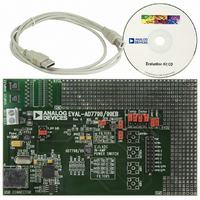
Manufacturer Part Number
EVAL-AD7799EBZ
Description
BOARD EVALUATION FOR AD7799
Manufacturer
Analog Devices Inc
Specifications of EVAL-AD7799EBZ
Number Of Adc's
1
Number Of Bits
24
Sampling Rate (per Second)
470
Data Interface
Serial
Inputs Per Adc
3 Differential
Input Range
±VREF/gain
Power (typ) @ Conditions
2.5mW @ 470SPS
Voltage Supply Source
Analog and Digital
Operating Temperature
-40°C ~ 105°C
Utilized Ic / Part
AD7799
Lead Free Status / RoHS Status
Lead free / RoHS Compliant


AD7798/AD7799
Parameter
REFERENCE
LOW-SIDE POWER SWITCH
DIGITAL OUTPUTS (P1 and P2)
INTERNAL CLOCK
LOGIC INPUTS
LOGIC OUTPUTS
External REFIN Voltage
Reference Voltage Range
Absolute REFIN Voltage Limits
Average Reference Input Current
Average Reference Input Current Drift
Normal Mode Rejection
Common-Mode Rejection
Reference Detect Levels
R
Allowable Current
Output High Voltage, V
Output Low Voltage, V
Output High Voltage, V
Output Low Voltage, V
Frequency
CS
SCLK and DIN
Input Currents
Input Capacitance
Output High Voltage, V
Output Low Voltage, V
Output High Voltage, V
Output Low Voltage, V
Floating-State Leakage Current
Floating-State Output Capacitance
Data Output Coding
ON
Input Low Voltage, V
Input High Voltage, V
(Schmitt-Triggered Input)
V
V
V
V
V
V
2
T
T
T
T
T
T
(+)
(–)
(+) – V
(+)
(–)
(+) − V
2
T
T
(–)
(–)
2
OL
OL
OL
OL
OH
OH
INL
OH
OH
INH
2
2
2
2
2
2
2
2
2
2
2
0.4
AD7798B/AD7799B
2.5
0.1
AV
GND − 30 mV
AV
400
±0.03
Same as for analog
inputs
100
0.3
0.65
7
9
30
AV
4
0.4
64 ± 3%
0.8
0.4
2.0
1.4/2
0.8/1.7
0.1/0.17
0.9/2
0.4/1.35
0.06/0.13
±10
10
DV
0.4
4
0.4
±10
10
Offset binary
DD
DD
DD
DD
+ 30 mV
− 0.6
− 0.6
Rev. A | Page 4 of 28
1
Unit
V nom
V min
V max
V min
V max
nA/V typ
nA/V/°C typ
dB typ
V min
V max
Ω max
Ω max
mA max
V min
V max
V min
V max
kHz min/max
V max
V max
V min
V min/max
V min/max
V min/max
V min/max
V min/max
V min/max
μA max
pF typ
V min
V max
V min
V max
μA max
pF typ
Test Conditions/Comments
REFIN = REFIN(+) − REFIN(−)
When V
limited to (0.9 x V
NOXREF bit active if V
AV
AV
Continuous current
AV
AV
AV
AV
DV
DV
DV
DV
DV
DV
DV
DV
DV
V
All digital inputs
DV
DV
DV
DV
IN
DD
DD
DD
DD
DD
DD
DD
DD
DD
DD
DD
DD
DD
DD
DD
DD
DD
DD
DD
= DV
= 5 V
= 3 V
= 3 V, I
= 3 V, I
= 5 V, I
= 5 V, I
= 5 V
= 3 V
= 3 V or 5 V
= 5 V
= 5 V
= 5 V
= 3 V
= 3 V
= 3 V
= 3 V, I
= 3 V, I
= 5 V, I
= 5 V, I
REF
DD
= AV
or GND
SOURCE
SINK
SOURCE
SINK
SOURCE
SINK
SOURCE
SINK
= 100 μA
= 800 μA
DD
= 100 μA
= 1.6 mA
, the differential input must be
= 100 μA
= 200 μA
REF
= 100 μA
= 200 μA
/gain) if the in-amp is active.
REF
< 0.3 V
Related parts for EVAL-AD7799EBZ
Image
Part Number
Description
Manufacturer
Datasheet
Request
R


Part Number:
Description:
BOARD EVAL FOR SI270X-A
Manufacturer:
Silicon Laboratories Inc
Datasheet:

Part Number:
Description:
BUCK CONV REF DESIGN KIT IP1201
Manufacturer:
International Rectifier
Datasheet:
Part Number:
Description:
BOARD DEMO SYNC DUAL BUCK CNVTER
Manufacturer:
International Rectifier
Datasheet:
Part Number:
Description:
BOARD DEMO SYNC BUCK CONVETER
Manufacturer:
International Rectifier
Datasheet:

Part Number:
Description:
EVALBOARD/EB Omnidirectional microphone - Analog
Manufacturer:
Analog Devices
Datasheet:
Part Number:
Description:
EVALBOARD/EB Omnidirectional microphone - Analog
Manufacturer:
Analog Devices
Datasheet:


Part Number:
Description:
BOARD EVAL LED DRIVER LT3756
Manufacturer:
Linear Technology
Datasheet:

Part Number:
Description:
BOARD EVAL FOR AD7741/7742
Manufacturer:
Analog Devices Inc
Datasheet:

Part Number:
Description:
±1.7g Dual-Axis IMEMS Accelerometer Evaluation Board
Manufacturer:
Analog Devices Inc
Datasheet:

Part Number:
Description:
IC MULTIPLIER ANALOG 8-SOIC T/R
Manufacturer:
Analog Devices Inc
Datasheet:

Part Number:
Description:
IC ANALOG MULTIPLIER 8-DIP
Manufacturer:
Analog Devices Inc
Datasheet:
Part Number:
Description:
IC ANALOG MULTIPLIER 8-SOIC
Manufacturer:
Analog Devices Inc
Datasheet:
Part Number:
Description:
IC ANALOG MULTIPLIER 8-DIP
Manufacturer:
Analog Devices Inc
Datasheet: