EVAL-AD7799EBZ Analog Devices Inc, EVAL-AD7799EBZ Datasheet - Page 5
EVAL-AD7799EBZ
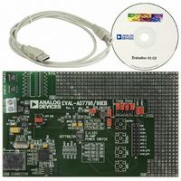
Manufacturer Part Number
EVAL-AD7799EBZ
Description
BOARD EVALUATION FOR AD7799
Manufacturer
Analog Devices Inc
Specifications of EVAL-AD7799EBZ
Number Of Adc's
1
Number Of Bits
24
Sampling Rate (per Second)
470
Data Interface
Serial
Inputs Per Adc
3 Differential
Input Range
±VREF/gain
Power (typ) @ Conditions
2.5mW @ 470SPS
Voltage Supply Source
Analog and Digital
Operating Temperature
-40°C ~ 105°C
Utilized Ic / Part
AD7799
Lead Free Status / RoHS Status
Lead free / RoHS Compliant


Parameter
SYSTEM CALIBRATION
POWER REQUIREMENTS
1
2
3
4
5
6
7
Temperature range is –40°C to +105°C. At the 19.6 Hz and 39.2 Hz update rates, the INL, power supply rejection (PSR), common-mode rejection (CMR), and normal
mode rejection (NMR) do not meet the data sheet specification if the voltage on the AIN(+) or AIN(−) pins exceeds AV
exceeded, the INL, for example, is reduced to 18 ppm of FS typically and the PSR is reduced to 69 dB typically. Therefore, for guaranteed performance at these update
rates, the absolute voltage on the analog input pins needs to be below AV
Specification is not production tested, but is supported by characterization data at initial product release.
Following a calibration, this error is in the order of the noise for the programmed gain and update rate selected.
Recalibration at any temperature removes these errors.
Full-scale error applies to both positive and negative full-scale and applies at the factory calibration conditions (AV
FS[3:0] are the four bits used in the mode register to select the output word rate.
Digital inputs equal to DV
Full-Scale Calibration Limit
Zero-Scale Calibration Limit
Input Span
Power Supply Voltage
Power Supply Currents
AV
DV
I
I
DD
DD
DD
DD
Current
(Power-Down Mode)
– GND
– GND
2
DD
7
or GND.
AD7798B/AD7799B
1.05 × FS
−1.05 × FS
0.8 × FS
2.1 × FS
2.7/5.25
2.7/5.25
140
180
400
500
1
Rev. A | Page 5 of 28
DD
1
− 1.6 V.
V min/max
μA max
Unit
V max
V min
V min
V max
V min/max
μA max
μA max
μA max
μA max
Test Conditions/Comments
FS = Full-scale analog input. When V
differential input must be limited to (0.9 × V
if the in-amp is active.
Unbuffered mode, 110 μA typ @ AV
125 μA typ @ AV
Buffered mode, gain = 1 or 2, 130 μA typ @ AV
165 μA typ @ AV
AD7798: gain = 4 to 128, 300 μA typ @ AV
350 μA typ @ AV
AD7799: gain = 4 to 128, 380 μA typ @ AV
440 μA typ @ AV
DD
= 4 V, gain = 1, T
DD
− 1.6 V typically. When this voltage is
DD
DD
DD
DD
= 5 V
= 5 V
= 5 V
= 5 V
A
= 25°C).
AD7798/AD7799
DD
REF
= 3 V,
= AV
REF
DD
DD
/gain)
DD
= 3 V,
= 3 V,
DD
, the
= 3 V,
Related parts for EVAL-AD7799EBZ
Image
Part Number
Description
Manufacturer
Datasheet
Request
R


Part Number:
Description:
BOARD EVAL FOR SI270X-A
Manufacturer:
Silicon Laboratories Inc
Datasheet:

Part Number:
Description:
BUCK CONV REF DESIGN KIT IP1201
Manufacturer:
International Rectifier
Datasheet:
Part Number:
Description:
BOARD DEMO SYNC DUAL BUCK CNVTER
Manufacturer:
International Rectifier
Datasheet:
Part Number:
Description:
BOARD DEMO SYNC BUCK CONVETER
Manufacturer:
International Rectifier
Datasheet:

Part Number:
Description:
EVALBOARD/EB Omnidirectional microphone - Analog
Manufacturer:
Analog Devices
Datasheet:
Part Number:
Description:
EVALBOARD/EB Omnidirectional microphone - Analog
Manufacturer:
Analog Devices
Datasheet:


Part Number:
Description:
BOARD EVAL LED DRIVER LT3756
Manufacturer:
Linear Technology
Datasheet:

Part Number:
Description:
BOARD EVAL FOR AD7741/7742
Manufacturer:
Analog Devices Inc
Datasheet:

Part Number:
Description:
±1.7g Dual-Axis IMEMS Accelerometer Evaluation Board
Manufacturer:
Analog Devices Inc
Datasheet:

Part Number:
Description:
IC MULTIPLIER ANALOG 8-SOIC T/R
Manufacturer:
Analog Devices Inc
Datasheet:

Part Number:
Description:
IC ANALOG MULTIPLIER 8-DIP
Manufacturer:
Analog Devices Inc
Datasheet:
Part Number:
Description:
IC ANALOG MULTIPLIER 8-SOIC
Manufacturer:
Analog Devices Inc
Datasheet:
Part Number:
Description:
IC ANALOG MULTIPLIER 8-DIP
Manufacturer:
Analog Devices Inc
Datasheet: