DAK-71A Power Integrations, DAK-71A Datasheet - Page 21
DAK-71A
Manufacturer Part Number
DAK-71A
Description
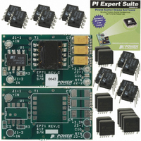
KIT DESIGN ACCELERATOR DC-DC
Manufacturer
Power Integrations
Series
DPA-Switch®r
Specifications of DAK-71A
Main Purpose
DC/DC, Step Down
Outputs And Type
1, Isolated
Voltage - Output
3.3V
Current - Output
2A
Voltage - Input
36 ~ 72V
Regulator Topology
Flyback
Frequency - Switching
400kHz
Board Type
Bare (Unpopulated) and Fully Populated
Utilized Ic / Part
DPA423, DPA424, DPA425
Lead Free Status / RoHS Status
Not applicable / Not applicable
Power - Output
-
Lead Free Status / Rohs Status
Lead free / RoHS Compliant
Other names
596-1009


www.powerint.com
Absolute Maximum Ratings
DRAIN Voltage .....................................................-0.3 V to 220 V
DRAIN Peak Current:
CONTROL Voltage ................................................ -0.3 V to 9 V
CONTROL Current .........................................................100 mA
LINE SENSE Pin Voltage ...................................... -0.3 V to 9 V
EXTERNAL CURRENT LIMIT Pin Voltage ........ -0.3 V to 9 V
FREQUENCY Pin Voltage ....................................... -0.3 V to 9 V
Theraml Impedance
Thermal Impedance: P or G Package:
Switching
Frequency
Duty Cycle (Prior to
Cycle Skipping)
Maximum Duty Cycle
Control Current at Start
of Cycle Skipping
External Bias
Current
Control Functions
Parameter
(θ
(θ
(θ
(θ
(θ
JA
JC
JA
JA
JC
) ........................... 70 °C/W
) .................................................40 °C/W
) .................................................30 °C/W
)
)
(3)
R Package:
(6)
............................................11 °C/W
................................................2 °C/W
DPA426....................................... 9.6 A
DPA422......................................1.31 A
DPA423......................................1.75 A
DPA424....................................... 3.5 A
DPA425...........................................7 A
Symbol
DC
(1,5)
DC
I
C(skip)
f
OSC
I
B
MAX
MIN
T
J
T
T
SOURCE = 0 V; T
I
C
J
J
= 25 °C
= 25 °C; f
= 25 °C; f
= I
(Unless Otherwise Specifi ed)
(1)
CD1
; 60 °C/W
See Figure 33
OSC
OSC
Conditions
Connected to CONTROL
Connected to SOURCE
= 400 kHz
= 400 kHz
(2)
FREQUENCY Pin
FREQUENCY Pin
(4)
(5)
J
= -40 to 125 °C
I
I
L
L
Storage Temperature-65 °C to 150 °C
Operating Junction Temperature
Lead Temperature
Notes:
1. All voltages referenced to SOURCE, T
2. Normally limited by internal circuitry.
3. 1/16” from case for 5 seconds.
4. Maximum ratings specifi ed may be applied, one at a time,
Notes:
1. Soldered to 0.36 sq. in. (232 mm
2. Soldered to 1 sq. in. (645 mm
3. Measured on pin 7 (SOURCE) close to plastic interface.
4. Soldered to 1 sq. in. (645 mm
5. Soldered to 3 sq. in. (1935 mm
6. Measured at the back surface of tab.
V
= 115 μA
= 80 μA
L
= 0 V
without causing permanent damage to the product.
Exposure to Absolute Maximum Rating conditions for
extended periods of time may affect product reliability.
DPA422
DPA423
DPA424
DPA425
DPA426
DPA422
DPA423
DPA424
DPA425
DPA426
(3)
....................................................... 260 °C
Min
375
282
1.8
2.5
3.6
4.4
71
52
32
2
(2)
2
2
2
), 2 oz. (610 g/m
), 2 oz. (610 g/m
), 2 oz. (610 g/m
.................... -40 °C to 150 °C
2
10.0
11.5
), 2 oz. (610 g/m
Typ
400
300
6.3
7.2
8.2
2.5
2.8
3.5
4.8
5.7
75
62
42
DPA422-426
4
A
= 25 °C.
Max
10.0
12.0
14.0
425
317
8.0
9.0
3.1
3.5
4.4
6.0
7.1
79
71
57
6
2
2
2
) copper clad.
) copper clad.
2
) copper clad.
) copper clad.
Units
Rev. S 12/07
kHz
mA
mA
%
%
21
Related parts for DAK-71A
Image
Part Number
Description
Manufacturer
Datasheet
Request
R

Part Number:
Description:
KIT DESIGN ACCELERATOR APPLIANCE
Manufacturer:
Power Integrations
Datasheet:

Part Number:
Description:
KIT DESIGN ACCELERATOR MODEM
Manufacturer:
Power Integrations
Datasheet:

Part Number:
Description:
KIT DESIGN ACCELERATOR SET TOP
Manufacturer:
Power Integrations
Datasheet:

Part Number:
Description:
KIT REF DES DPA 6.6W DC-DC CONV
Manufacturer:
Power Integrations
Datasheet:

Part Number:
Description:
KIT DESIGN ACCELERATOR POE CONV
Manufacturer:
Power Integrations
Datasheet:

Part Number:
Description:
DESIGN ACCELERATOR KIT XT SWITCH
Manufacturer:
Power Integrations
Datasheet:

Part Number:
Description:
DESIGN ACCELERATOR KIT LP SWITCH
Manufacturer:
Power Integrations
Datasheet:

Part Number:
Description:
KIT DESIGN ACC PEAKSWITCH FAMILY
Manufacturer:
Power Integrations
Datasheet:

Part Number:
Description:
KIT DESIGN ACCELERATOR ADAPTER
Manufacturer:
Power Integrations
Datasheet:

Part Number:
Description:
KIT DESIGN ACCELERATOR ADAPTER
Manufacturer:
Power Integrations
Datasheet: