DAK-71A Power Integrations, DAK-71A Datasheet - Page 6
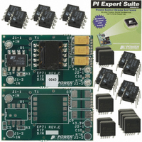
DAK-71A
Manufacturer Part Number
DAK-71A
Description
KIT DESIGN ACCELERATOR DC-DC
Manufacturer
Power Integrations
Series
DPA-Switch®r
Specifications of DAK-71A
Main Purpose
DC/DC, Step Down
Outputs And Type
1, Isolated
Voltage - Output
3.3V
Current - Output
2A
Voltage - Input
36 ~ 72V
Regulator Topology
Flyback
Frequency - Switching
400kHz
Board Type
Bare (Unpopulated) and Fully Populated
Utilized Ic / Part
DPA423, DPA424, DPA425
Lead Free Status / RoHS Status
Not applicable / Not applicable
Power - Output
-
Lead Free Status / Rohs Status
Lead free / RoHS Compliant
Other names
596-1009


Rev. S 12/07
The maximum duty cycle, DC
value of 75% (typical). However, by connecting the LINE-SENSE
to the DC input bus through a resistor with appropriate value,
the maximum duty cycle can be made to decrease from 75% to
33% (typical) as shown in Figure 7 when input line voltage
increases (see Line Feed-Forward with DC
Minimum Duty Cycle and Cycle Skipping
To maintain power supply output regulation, the pulse width
modulator reduces duty cycle as the load at the power supply
output decreases. This reduction in duty cycle is proportional to
the current fl owing into the CONTROL pin. As the CONTROL
pin current increases, the duty cycle reduces linearly towards a
minimum value specifi ed as minimum duty cycle, DC
reaching DC
approximately 2 mA, the pulse width modulator will force the
duty cycle from DC
4). This feature allows a power supply to operate in a cycle
skipping mode when the load consumes less power than the
DPA-Switch delivers at minimum duty cycle, DC
additional control is needed for the transition between normal
operation and cycle skipping. As the load increases or
decreases, the power supply automatically switches between
normal and cycle skipping mode as necessary.
Cycle skipping may be avoided, if so desired, by connecting a
minimum load at the power supply output such that the duty
cycle remains at a level higher than DC
Error Amplifi er
The shunt regulator can also perform the function of an error
amplifi er in primary side feedback applications. The shunt
regulator voltage is accurately derived from a temperature-
compensated bandgap reference. The gain of the error amplifi er
is set by the CONTROL pin dynamic impedance. The
CONTROL pin clamps external circuit signals to the V
level. The CONTROL pin current in excess of the supply current
is separated by the shunt regulator and fl ows through R
voltage error signal.
On-chip Current Limit with External Programmability
The cycle-by-cycle peak drain current limit circuit uses the
output MOSFET ON-resistance as a sense resistor. A current
limit comparator compares the output MOSFET on-state drain
to source voltage, V
limit, V
turned off until the start of the next clock cycle. The current limit
comparator threshold voltage is temperature compensated to
minimize the variation of the current limit due to temperature
related changes in R
current limit of DPA-Switch is preset internally. However, with a
resistor connected between EXTERNAL CURRENT LIMIT pin
and SOURCE pin, the current limit can be programmed
externally to a lower level between 25% and 100% of the default
current limit. Please refer to the graphs in the Typical
Performance Characteristics section for the selection of the
resistor value. By setting current limit low, a larger DPA-Switch
than necessary for the power required can be used to take
advantage of the lower R
sinking requirements. With a second resistor connected
between the EXTERNAL CURRENT LIMIT pin and the DC input
6
DS(ON)
exceeds the threshold voltage and the MOSFET is
DPA422-426
MIN
, if CONTROL pin current is increased further by
MIN
DS(ON)
DS(ON)
to zero in a discrete step (refer to Figure
with a threshold voltage. At the current
DS(ON)
of the output MOSFET. The default
MAX
for higher effi ciency/smaller heat
is set at a default maximum
MIN
at all times.
MAX
Reduction).
MIN
. No
MIN
C
voltage
. After
E
as a
bus, the current limit is reduced with increasing line voltage,
allowing a true power limiting operation against line variation to
be implemented in a fl yback confi guration.
The leading edge blanking circuit inhibits the current limit
comparator for a short time after the output MOSFET is turned
on. The leading edge blanking time has been set so that, if a
power supply is designed properly, current spikes caused by
primary-side capacitance and secondary-side rectifi er reverse
recovery time should not cause premature termination of the
switching pulse.
The current limit after the leading edge blanking time is as
shown in Figure 31. To avoid triggering the current limit in
normal operation, the drain current waveform should stay within
the envelope shown.
Line Under-Voltage Detection (UV)
At power up, UV keeps DPA-Switch off until the input line
voltage reaches the under voltage upper threshold. At power
down, UV holds DPA-Switch on until the input voltage falls
below the under voltage lower threshold. A single resistor
connected from the LINE-SENSE pin to the DC input bus sets
UV upper and lower thresholds. To avoid false triggering by
noise, a hysteresis is implemented which sets the UV lower
threshold typically at 94% of the UV upper threshold. If the UV
lower threshold is reached during operation without the power
supply losing regulation and the condition stays longer than
10 μs (typical), the device will turn off and stay off until the UV
upper threshold has been reached again. Then, a soft-start will
be initiated the next time CONTROL pin voltage reaches 5.8.V. If
the power supply loses regulation before reaching the UV lower
threshold, the device will enter auto-restart. At the end of each
auto-restart cycle (S7), the UV comparator is enabled. If the UV
upper threshold is not exceeded, the MOSFET will be disabled
during the next cycle (see Figure 5). The UV feature can be
disabled independent of OV feature.
Line Overvoltage Shutdown (OV)
The same resistor used for UV also sets an overvoltage
threshold which, once exceeded, will force the DPA-Switch
output into the off-state within one switching cycle. The ratio of
OV and UV thresholds is preset at 2.7 as can be seen in
Figure 7. When the MOSFET is off, the input voltage surge
capability is increased to the voltage rating of the MOSFET
(220 V), due to the absence of the refl ected voltage and leakage
spikes on the drain. A small amount of hysteresis is provided on
the OV threshold to prevent noise triggering. The OV feature
can be disabled independent of the UV feature as shown in
Figure 13.
Line Feed-Forward with DC
The same resistor used for UV and OV also implements line
voltage feed-forward that minimizes output line ripple and
reduces power supply output sensitivity to line transients. This
feed-forward operation is illustrated in Figure 4 by the different
values of I
higher line voltage results in smaller operating duty cycle. As an
added feature, the maximum duty cycle DC
from 75% (typical) at a voltage slightly higher than the UV
threshold to 33% (typical) at the OV threshold
L
. Note that for the same CONTROL pin current,
MAX
Reduction
MAX
www.powerint.com
is also reduced
Related parts for DAK-71A
Image
Part Number
Description
Manufacturer
Datasheet
Request
R

Part Number:
Description:
KIT DESIGN ACCELERATOR APPLIANCE
Manufacturer:
Power Integrations
Datasheet:

Part Number:
Description:
KIT DESIGN ACCELERATOR MODEM
Manufacturer:
Power Integrations
Datasheet:

Part Number:
Description:
KIT DESIGN ACCELERATOR SET TOP
Manufacturer:
Power Integrations
Datasheet:

Part Number:
Description:
KIT REF DES DPA 6.6W DC-DC CONV
Manufacturer:
Power Integrations
Datasheet:

Part Number:
Description:
KIT DESIGN ACCELERATOR POE CONV
Manufacturer:
Power Integrations
Datasheet:

Part Number:
Description:
DESIGN ACCELERATOR KIT XT SWITCH
Manufacturer:
Power Integrations
Datasheet:

Part Number:
Description:
DESIGN ACCELERATOR KIT LP SWITCH
Manufacturer:
Power Integrations
Datasheet:

Part Number:
Description:
KIT DESIGN ACC PEAKSWITCH FAMILY
Manufacturer:
Power Integrations
Datasheet:

Part Number:
Description:
KIT DESIGN ACCELERATOR ADAPTER
Manufacturer:
Power Integrations
Datasheet:

Part Number:
Description:
KIT DESIGN ACCELERATOR ADAPTER
Manufacturer:
Power Integrations
Datasheet: