CDB43L21 Cirrus Logic Inc, CDB43L21 Datasheet - Page 2
CDB43L21
Manufacturer Part Number
CDB43L21
Description
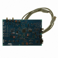
BOARD EVAL FOR CS43L21 DAC
Manufacturer
Cirrus Logic Inc
Datasheet
1.CDB-43L21.pdf
(25 pages)
Specifications of CDB43L21
Description/function
Audio D/A
Operating Supply Voltage
5 V
Product
Audio Modules
For Use With/related Products
CS43L21
Lead Free Status / RoHS Status
Contains lead / RoHS non-compliant
Lead Free Status / RoHS Status
Lead free / RoHS Compliant, Contains lead / RoHS non-compliant
Other names
598-1528


2
TABLE OF CONTENTS
1. SYSTEM OVERVIEW ............................................................................................................................. 4
2. SOFTWARE MODE CONTROL ............................................................................................................. 7
3. HARDWARE MODE CONTROL .......................................................................................................... 11
4. SYSTEM CONNECTIONS .................................................................................................................... 14
5. JUMPER SETTINGS ............................................................................................................................ 14
6. CDB43L21 BLOCK DIAGRAM ............................................................................................................ 15
7. CS43L21 SCHEMATICS ...................................................................................................................... 16
8. CDB43L21 LAYOUT ............................................................................................................................ 22
9. ERRATA ............................................................................................................................................... 25
10. REVISION HISTORY .......................................................................................................................... 25
1. SYSTEM OVERVIEW ............................................................................................................................. 4
2. SOFTWARE MODE CONTROL ............................................................................................................. 7
3. HARDWARE MODE CONTROL .......................................................................................................... 11
4. SYSTEM CONNECTIONS .................................................................................................................... 14
5. JUMPER SETTINGS ............................................................................................................................ 14
6. CDB43L21 BLOCK DIAGRAM ............................................................................................................ 15
7. CS43L21 SCHEMATICS ...................................................................................................................... 16
8. CDB43L21 LAYOUT ............................................................................................................................ 22
1.1 Power ............................................................................................................................................... 4
1.2 Grounding and Power Supply Decoupling ....................................................................................... 4
1.3 FPGA ............................................................................................................................................... 4
1.4 CS43L21 .......................................................................................................................................... 4
1.5 CS8415 Digital Audio Receiver ........................................................................................................ 5
1.6 Oscillator .......................................................................................................................................... 5
1.7 I/O Stake Headers ........................................................................................................................... 5
1.8 Analog Outputs ................................................................................................................................ 5
1.9 Stand-Alone Switches ...................................................................................................................... 6
1.10 Control Port Connectors ................................................................................................................ 6
2.1 General Configuration Tab ............................................................................................................... 8
2.2 DAC Volume Controls Tab ............................................................................................................... 9
2.3 Register Maps Tab ......................................................................................................................... 10
3.1 FPGA H/W Control ......................................................................................................................... 11
3.2 CS43L21 H/W Control ................................................................................................................... 11
1.10.1 USB Connector ..................................................................................................................... 6
1.10.2 RS-232 Connector ................................................................................................................. 6
1.10.1 USB Connector ..................................................................................................................... 6
1.10.2 RS-232 Connector ................................................................................................................. 6
CDB43L21
DS723DB1
Related parts for CDB43L21
Image
Part Number
Description
Manufacturer
Datasheet
Request
R

Part Number:
Description:
EVAL BOARD FOR CS43L21
Manufacturer:
Cirrus Logic Inc
Datasheet:

Part Number:
Description:
Development Kit
Manufacturer:
Cirrus Logic Inc
Datasheet:
Part Number:
Description:
Development Kit
Manufacturer:
Cirrus Logic Inc
Datasheet:


Part Number:
Description:
High-efficiency PFC + Fluorescent Lamp Driver Reference Design
Manufacturer:
Cirrus Logic Inc
Datasheet:
Part Number:
Description:
Development Kit
Manufacturer:
Cirrus Logic Inc
Datasheet:
Part Number:
Description:
Development Kit
Manufacturer:
Cirrus Logic Inc
Datasheet:

Part Number:
Description:
Development Kit
Manufacturer:
Cirrus Logic Inc
Datasheet:
Part Number:
Description:
Development Kit
Manufacturer:
Cirrus Logic Inc
Datasheet:
Part Number:
Description:
Development Kit
Manufacturer:
Cirrus Logic Inc
Datasheet:

Part Number:
Description:
EVALUATION BOARD FOR CS8427
Manufacturer:
Cirrus Logic Inc
Datasheet:

Part Number:
Description:
BOARD EVAL FOR CS8416 RCVR
Manufacturer:
Cirrus Logic Inc
Datasheet:

Part Number:
Description:
EVALUATION BOARD FOR CS8420
Manufacturer:
Cirrus Logic Inc
Datasheet:

Part Number:
Description:
KIT DEVELOPMENT EP9315 ARM9
Manufacturer:
Cirrus Logic Inc
Datasheet:

Part Number:
Description:
KIT DEVELOPMENT EP9302 ARM9
Manufacturer:
Cirrus Logic Inc
Datasheet: