RDK-131 Power Integrations, RDK-131 Datasheet - Page 7
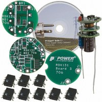
RDK-131
Manufacturer Part Number
RDK-131
Description
KIT REF DESIGN LED LINKSWITCH TN
Manufacturer
Power Integrations
Series
LinkSwitch-TNr
Specifications of RDK-131
Current - Output / Channel
300mA
Outputs And Type
1, Non-Isolated
Voltage - Output
10V
Features
fits within GU10 lamp base
Voltage - Input
85 ~ 265VAC
Utilized Ic / Part
LNK306DN
Lead Free Status / RoHS Status
Not applicable / Not applicable
Other names
596-1127


7-Mar-07
RDR-131 LED Driver – LNK306DN
4 Circuit Description
4.1 Configuration and Assembly Details
The power supply is configured as a non-isolated buck converter. Since it must fit in a
GU10 lamp socket base, the supply was split into 2 interconnected boards. A Faraday
shield (the third board) was sandwiched between the input rectification/EMI filter
(bottom) board and the converter (top) board. The shield board is electrically connected
to the converter board. This was necessary to meet the conducted EMI requirements.
The shield consists of a single-sided, copper-clad PCB that is the same size as the
input rectification/EMI filter board.
4.2 AC Input Rectification
A 10 Ω fusible resistor (RF1) will act as a fuse if a catastrophic failure occurs. The input
voltage and current are rectified by a bridge rectifier (BR1) and smoothed by a pi filter
circuit (C1, L1 and C2). The pi filter and RF1 also help attenuate the differential mode
conducted EMI that is generated by the switching of the buck converter.
4.3 LinkSwitch-TN
The PI Xls spreadsheet tool was used to design this converter. When powering the
designated LED load, the converter operates in the continuous conduction mode
(CCM). The buck converter stage consists of the integrated MOSFET switch within the
LNK306DN (U1), a freewheeling diode (D3), an output inductor (L2) and an output
capacitor (C3). An Ultrafast MURS160T3 was chosen for the freewheeling diode to
minimize the amplitude of the MOSFET turn-on spike. The remaining components are
involved in sensing the normal-load output current and the no-load output voltage and
conveying that information back to the FEEDBACK (FB) pin of the LNK306DN.
4.4 Output Feedback
The LinkSwitch-TN uses On/Off control to regulate the output of the supply. During
each enabled switching cycle the drain current ramps to a fixed internal current limit
level. When current into the FEEDBACK (FB) pin exceeds 49 µA the next switching is
disabled. By adjusting the number of enabled to disabled cycles the amount of energy
delivered to the output can be varied to maintain regulation. The 49 µA threshold is
specified at a FB pin voltage of 1.65 V allowing this pin to be used as a voltage
reference.
In this design both current and voltage feedback is used. Current feedback limits the
LED current during normal operation while voltage feedback limits the output voltage
should the LED load be disconnected, for example during production testing.
During the off time of U1, the voltage that appears across C2 is equal to the output
voltage less a diode drop. In this design two 250 V rated diodes, D1 and D2, were used
for space reasons, however a single 600 V diode could be used (in this case the voltage
across C2 would be equal to the output voltage).
Power Integrations
Tel: +1 408 414 9200 Fax: +1 408 414 9201
Page 7 of 24
www.powerint.com
Related parts for RDK-131
Image
Part Number
Description
Manufacturer
Datasheet
Request
R

Part Number:
Description:
KIT REF DESIGN FOR LNK457D
Manufacturer:
Power Integrations
Datasheet:

Part Number:
Description:
REFERENCE DESIGN LINKSWITCH-PH
Manufacturer:
Power Integrations
Datasheet:

Part Number:
Description:
KIT REF DESIGN FOR LNK403EG
Manufacturer:
Power Integrations
Datasheet:

Part Number:
Description:
KIT REF DESIGN FOR LNK406EG
Manufacturer:
Power Integrations
Datasheet:

Part Number:
Description:
KIT REF DESIGN LINKSWITCH-CV
Manufacturer:
Power Integrations
Datasheet:

Part Number:
Description:
KIT REF DESIGN LINKSWITCH 2
Manufacturer:
Power Integrations
Datasheet:

Part Number:
Description:
Specifications: Family: Eval Boards - DC/DC & AC/DC (Off-Line) SMPS ; Series: HiperLCS™ ; Main Purpose: DC/DC, Step Down ; Outputs and Type: 1, Isolated ; Power - Output: 150W ; Voltage - Output: 24V ; Current - Output: 6.25A ; Voltage - Input:
Manufacturer:
Power Integrations, Inc.
Datasheet:

Part Number:
Description:
KIT DESIGN REF TINYSWITCH-III
Manufacturer:
Power Integrations
Datasheet:

Part Number:
Description:
KIT DESIGN REF LINKSWITCH LP
Manufacturer:
Power Integrations
Datasheet:
Part Number:
Description:
KIT REF DESIGN PG LINKSWITCH-II
Manufacturer:
Power Integrations
Datasheet:
Part Number:
Description:
REFERENCE DESIGN LINKSWITCH-PL
Manufacturer:
Power Integrations
Datasheet:
Part Number:
Description:
REFERENCE DESIGN LINKSWITCH-PH
Manufacturer:
Power Integrations
Datasheet:

Part Number:
Description:
KIT REF DESIGN 36-72W MOTOR DRVR
Manufacturer:
Power Integrations
Datasheet:
Part Number:
Description:
Specifications: Manufacturer: Power Integrations ; Output Voltage: 380 VDC ; Input / Supply Voltage (Max): 264 VAC ; Input / Supply Voltage (Min): 90 VAC ; Mounting Style: Through Hole ; Output Current: 0.913 A ; Output Power: 347 W
Manufacturer:
Power Integrations, Inc.

Part Number:
Description:
KIT REF DESIGN TOP HX FOR TOP258
Manufacturer:
Power Integrations
Datasheet: