LM3429BSTEVAL/NOPB National Semiconductor, LM3429BSTEVAL/NOPB Datasheet - Page 12
LM3429BSTEVAL/NOPB
Manufacturer Part Number
LM3429BSTEVAL/NOPB
Description
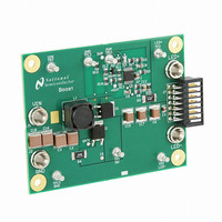
BOARD EVAL FOR BOOST LM3429
Manufacturer
National Semiconductor
Series
PowerWise®r
Specifications of LM3429BSTEVAL/NOPB
Current - Output / Channel
1A
Outputs And Type
1, Non-Isolated
Features
Dimmable
Voltage - Input
10 ~ 26 V
Utilized Ic / Part
LM3429
Core Chip
LM3429
Topology
Buck-Boost
No. Of Outputs
1
Dimming Control Type
PWM / Analog
Development Tool Type
Hardware - Eval/Demo Board
Mcu Supported Families
LM3429 Family
Msl
MSL 1 - Unlimited
Lead Free Status / RoHS Status
Lead free by exemption / RoHS compliant by exemption
Voltage - Output
-
Other names
*LM3429BSTEVAL
*LM3429BSTEVAL/NOPB
LM3429BSTEVAL
*LM3429BSTEVAL/NOPB
LM3429BSTEVAL
Available stocks
Company
Part Number
Manufacturer
Quantity
Price
Company:

Part Number:
LM3429BSTEVAL/NOPB
Manufacturer:
National Semiconductor
Quantity:
135


www.national.com
To mitigate this problem, a compensator should be designed
to give adequate phase margin (above 45°) at the crossover
frequency. A simple compensator using a single capacitor at
the COMP pin (C
which will ensure adequate phase margin if placed low
enough. At high duty cycles (as shown in
zero places extreme limits on the achievable bandwidth with
this type of compensation. However, because an LED driver
is essentially free of output transients (except catastrophic
failures open or short), the dominant pole approach, even with
reduced bandwidth, is usually the best approach. The domi-
nant compensation pole (ω
output resistance (R
It may also be necessary to add one final pole at least one
decade above the crossover frequency to attenuate switching
noise and, in some cases, provide better gain margin. This
pole can be placed across R
resistor at the same time.
sation is physically implemented in the system.
The high frequency pole (ω
The total system transfer function becomes:
The resulting compensated loop gain frequency response
shown in
phase margin (above 45°) if the dominant compensation pole
is placed low enough, ensuring stability:
FIGURE 9. Compensated Loop Gain Frequency
Figure 9
CMP
indicates that the system has adequate
O
) will add a dominant pole to the system,
) of the error amplifier (typically 5 MΩ):
Response
Figure 8
P2
P3
SNS
) is determined by C
) can be calculated:
to filter the ESL of the sense
shows how the compen-
Figure
7), the RHP
CMP
300944a4
and the
12
OUTPUT OVER-VOLTAGE LOCKOUT (OVLO)
The LM3429 can be configured to detect an output (or input)
over-voltage condition via the OVP pin. The pin features a
precision 1.24V threshold with 20 µA (typical) of hysteresis
current as shown in
exceeded, the GATE pin is immediately pulled low and a 20
µA current source provides hysteresis to the lower threshold
of the OVLO hysteretic band.
If the LEDs are referenced to a potential other than ground
(floating), as in the buck-boost and buck configuration, the
output voltage (V
ground by using a single PNP as shown in
The over-voltage turn-off threshold (V
follows:
Ground Referenced
Floating
In the ground referenced configuration, the voltage across
R
V
transistor.
The over-voltage hysteresis (V
O
OV2
- 620 mV where 620 mV approximates the V
is V
FIGURE 10. Over-Voltage Protection Circuitry
FIGURE 11. Floating Output OVP Circuitry
O
- 1.24V whereas in the floating configuration it is
O
) should be sensed and translated to
Figure
10. When the OVLO threshold is
HYSO
) is defined as follows:
TURN-OFF
30094459
Figure
) is defined as
BE
of the PNP
11.
30094458
Related parts for LM3429BSTEVAL/NOPB
Image
Part Number
Description
Manufacturer
Datasheet
Request
R

Part Number:
Description:
National Semiconductor [8-Bit D/A Converter]
Manufacturer:
National Semiconductor
Datasheet:
Part Number:
Description:
National Semiconductor [Media Coprocessor]
Manufacturer:
National Semiconductor
Datasheet:
Part Number:
Description:
Digitally Controlled Tone and Volume Circuit with Stereo Audio Power Amplifier, Microphone Preamp Stage and National 3D Sound
Manufacturer:
National Semiconductor
Datasheet:
Part Number:
Description:
Digitally Controlled Tone and Volume Circuit with Stereo Audio Power Amplifier, Microphone Preamp Stage and National 3D Sound
Manufacturer:
National Semiconductor
Datasheet:
Part Number:
Description:
AC97 Rev 2 Codec with Sample Rate Conversion and National 3D Sound
Manufacturer:
National Semiconductor
Part Number:
Description:
Manufacturer:
National Semiconductor
Datasheet:
Part Number:
Description:
Manufacturer:
National Semiconductor
Datasheet:
Part Number:
Description:
General Purpose, Low Voltage, Low Power, Rail-to-Rail Output Operational Amplifiers
Manufacturer:
National Semiconductor
Datasheet:
Part Number:
Description:
8-bit 20 MSPS flash A/D converter.
Manufacturer:
National Semiconductor
Datasheet:
Part Number:
Description:
Low Noise Quad Operational Amplifier
Manufacturer:
National Semiconductor
Datasheet:
Part Number:
Description:
Quad Differential Line Receivers
Manufacturer:
National Semiconductor
Datasheet:
Part Number:
Description:
Quad High Speed Trapezoidal? Bus Transceiver
Manufacturer:
National Semiconductor
Datasheet:
Part Number:
Description:
Dual Line Receiver
Manufacturer:
National Semiconductor
Datasheet:
Part Number:
Description:
TTL to 10k ECL Level Translator with Latch
Manufacturer:
National Semiconductor
Datasheet: