MCP651EV-VOS Microchip Technology, MCP651EV-VOS Datasheet - Page 27
MCP651EV-VOS
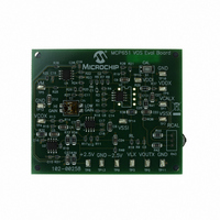
Manufacturer Part Number
MCP651EV-VOS
Description
BOARD EVAL OP AMP MCP651
Manufacturer
Microchip Technology
Series
mCal Technologyr
Specifications of MCP651EV-VOS
Channels Per Ic
1 - Single
Amplifier Type
General Purpose
Output Type
Single-Ended, Rail-to-Rail
Slew Rate
30 V/µs
Current - Output / Channel
100mA
Operating Temperature
-40°C ~ 125°C
Current - Supply (main Ic)
6mA
Voltage - Supply, Single/dual (±)
2.5 V ~ 5.5 V
Board Type
Fully Populated
Utilized Ic / Part
MCP651
Processor To Be Evaluated
MCP651
Maximum Operating Temperature
+ 125 C
Minimum Operating Temperature
- 40 C
Operating Supply Voltage
2.5 V to 5.5 V
Tool Type
Evaluation Board
Core Architecture
PIC
Cpu Core
PIC
Data Bus Width
8 bit
Lead Free Status / RoHS Status
Lead free / RoHS Compliant
-3db Bandwidth
-
Lead Free Status / Rohs Status
Lead free / RoHS Compliant
Available stocks
Company
Part Number
Manufacturer
Quantity
Price
Company:

Part Number:
MCP651EV-VOS
Manufacturer:
Microchip Technology
Quantity:
135
Company:
Part Number:
MCP651EV-VOS
Manufacturer:
MICROCHIP
Quantity:
12 000


4.3.9.3
Figure 4-12
fier circuit. Usually, we choose R
The guard traces (with ground vias at the ends) help
minimize the thermal gradients. The resistor layout
cancels the resistor thermal voltages, assuming the
temperature gradient is constant near the resistors:
EQUATION 4-3:
FIGURE 4-12:
for Single Difference Amplifier.
© 2008 Microchip Technology Inc.
Where:
Thermal voltages are approximately equal
Note:
V
G
V
M
P
DM
V
V
M
P
Changing the orientation of the resistors
will usually cause a significant decrease in
the cancellation of the thermal voltages.
shows the recommended difference ampli-
V
V
=
MCP6V01
Difference Amplifier Layout for
Thermo-junctions
OUT
OUT
R4
R2
R1
R3
R
V
R
≈ V
≈ V
R
3
OS
1
2
/R
U
REF
REF
is neglected
1
1
PCB Layout and Schematic
= R
+ (V
+ (V
4
R
R
/R
P
P
4
3
U1
2
– V
– V
, difference gain
1
= R
M
M
V
)G
)G
2
REF
DM
DM
V
and R
OUT
V
V
3
OUT
REF
= R
4
.
4.3.9.4
The dual op amp amplifiers shown in
Figure 4-17
greater than 1, and a common mode gain of 1 .They
can use the layout shown in
ting resistors (R
bined so that the thermal voltages can be canceled.
The guard traces (with ground vias at the ends) help
minimize the thermal gradients. The resistor layout
cancels the resistor thermal voltages, assuming the
temperature gradient is constant near the resistors:
EQUATION 4-4:
FIGURE 4-13:
for Dual Non-inverting Amplifier.
Where:
Thermal voltages are approximately equal
Note:
G
G
R3
R2
R1
DM
CM
V
V
IA
IB
=
=
Changing the orientation of the resistors
will usually cause a significant decrease in
the cancellation of the thermal voltages.
(V
(V
produce a non-inverting difference gain
Dual Non-inverting Amplifier Layout
for Thermo-junctions
½ MCP6V02
½ MCP6V02
OA
OA
1 + R
1, common mode gain
V
2
) between the two sides are not com-
OS
– V
+ V
V
MCP6V01/2/3
is neglected
3
OB
OA
OB
R
R
R
R
/R
V
PCB Layout and Schematic
1
1
2
2
IA
U1
) ≈ (V
)/2 ≈ (V
2
U
U
, differential mode gain
1
1
V
Figure
IA
IB
IA
– V
R
R
V
3
3
+ V
OB
IB
4-13. The gain set-
DS22058C-page 27
)G
IB
Figure 4-16
)/2
DM
V
V
OA
OB
R3
R2
R1
and
Related parts for MCP651EV-VOS
Image
Part Number
Description
Manufacturer
Datasheet
Request
R

Part Number:
Description:
Manufacturer:
Microchip Technology Inc.
Datasheet:
Part Number:
Description:
Manufacturer:
Microchip Technology Inc.
Datasheet:
Part Number:
Description:
Manufacturer:
Microchip Technology Inc.
Datasheet:
Part Number:
Description:
Manufacturer:
Microchip Technology Inc.
Datasheet:
Part Number:
Description:
Manufacturer:
Microchip Technology Inc.
Datasheet:
Part Number:
Description:
Manufacturer:
Microchip Technology Inc.
Datasheet:
Part Number:
Description:
Manufacturer:
Microchip Technology Inc.
Datasheet:
Part Number:
Description:
Manufacturer:
Microchip Technology Inc.
Datasheet: