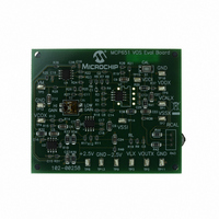
MCP651EV-VOS Microchip Technology, MCP651EV-VOS Datasheet - Page 29
MCP651EV-VOS
Manufacturer Part Number
MCP651EV-VOS
Description
BOARD EVAL OP AMP MCP651
Manufacturer
Microchip Technology
Series
mCal Technologyr
Specifications of MCP651EV-VOS
Channels Per Ic
1 - Single
Amplifier Type
General Purpose
Output Type
Single-Ended, Rail-to-Rail
Slew Rate
30 V/µs
Current - Output / Channel
100mA
Operating Temperature
-40°C ~ 125°C
Current - Supply (main Ic)
6mA
Voltage - Supply, Single/dual (±)
2.5 V ~ 5.5 V
Board Type
Fully Populated
Utilized Ic / Part
MCP651
Processor To Be Evaluated
MCP651
Maximum Operating Temperature
+ 125 C
Minimum Operating Temperature
- 40 C
Operating Supply Voltage
2.5 V to 5.5 V
Tool Type
Evaluation Board
Core Architecture
PIC
Cpu Core
PIC
Data Bus Width
8 bit
Lead Free Status / RoHS Status
Lead free / RoHS Compliant
-3db Bandwidth
-
Lead Free Status / Rohs Status
Lead free / RoHS Compliant
Available stocks
Company
Part Number
Manufacturer
Quantity
Price
Company:

Part Number:
MCP651EV-VOS
Manufacturer:
Microchip Technology
Quantity:
135
Company:
Part Number:
MCP651EV-VOS
Manufacturer:
MICROCHIP
Quantity:
12 000


4.4
4.4.1
Many sensors are configured as Wheatstone bridges.
Strain gauges and pressure sensors are two common
examples. These signals can be small and the
common mode noise large. Amplifier designs with high
differential gain are desirable.
Figure 4-15
bridge with a minimum of components. Because the
circuit is not symmetric, the ADC input is single ended,
and there is a minimum of filtering, the CMRR is good
enough for moderate common mode noise.
FIGURE 4-15:
Figure 4-16
Wheatstone bridges. This circuit is symmetric and has
high CMRR. Using a differential input to the ADC helps
with the CMRR.
FIGURE 4-16:
© 2008 Microchip Technology Inc.
R R
R R
R R
R R
V
Typical Applications
DD
WHEATSTONE BRIDGE
shows how to interface to a Wheatstone
shows a higher performance circuit for
10 nF
10 nF
V
DD
0.2R
0.2R
Simple Design.
High Performance Design.
1 µF
200Ω
200Ω
200 Ω
200 Ω
0.01C
100R
MCP6V01
20 kΩ
20 kΩ
3 kΩ
1 µF
1 µF
3 kΩ
3 kΩ
½ MCP6V02
½ MCP6V02
ADC
V
DD
ADC
V
DD
4.4.2
The ratiometric circuit in
wire RTD. It corrects for the sensor’s wiring resistance
by subtracting the voltage across the middle R
top R1 does not change the output voltage; it balances
the op amp inputs. Failure (open) of the RTD is
detected by an out of range voltage.
FIGURE 4-17:
The voltages at the input of the ADC can be calculated
with the following:
Where:
R
R
R
V
V
R
100Ω
W
W
W
V
V
CM
DM
V
G
RTD
W
V
V
B
T
RTD
G
DM
CM
W
RTD SENSOR
=
=
=
=
=
=
=
=
=
10 nF
10 nF
1
G
G
V
------------------------------------------------------------------------------
V
T
+
RTD
RTD
DD
+
MCP6V01/2/3
2 R
Voltage at the top of R
Voltage at the bottom of R
Voltage across top and middle
R
ADC’s common mode input
ADC’s differential mode input
R
20 kΩ
R
20 kΩ
V
⋅
(
W
–
T
B
V
RTD Sensor.
B
’s
1 µF
R
2.49 kΩ
2.49 kΩ
T
3
Figure 4-17
+
2.49 kΩ
2.49 kΩ
3
–
⁄
(
R
R
R
⁄
V
G
R
2
1
1
B
1
RTD
)
2
+
G
+
W
R
2.55 kΩ
R
2.55 kΩ
1 G
100 kΩ
100 kΩ
100 nF
100 nF
DS22058C-page 29
conditions a three
V
2
2
–
R
R
W
3
3
½ MCP6V02
½ MCP6V02
W
)V
RTD
W
RTD
3 kΩ
3 kΩ
ADC
W
V
. The
DD
Related parts for MCP651EV-VOS
Image
Part Number
Description
Manufacturer
Datasheet
Request
R

Part Number:
Description:
Manufacturer:
Microchip Technology Inc.
Datasheet:
Part Number:
Description:
Manufacturer:
Microchip Technology Inc.
Datasheet:
Part Number:
Description:
Manufacturer:
Microchip Technology Inc.
Datasheet:
Part Number:
Description:
Manufacturer:
Microchip Technology Inc.
Datasheet:
Part Number:
Description:
Manufacturer:
Microchip Technology Inc.
Datasheet:
Part Number:
Description:
Manufacturer:
Microchip Technology Inc.
Datasheet:
Part Number:
Description:
Manufacturer:
Microchip Technology Inc.
Datasheet:
Part Number:
Description:
Manufacturer:
Microchip Technology Inc.
Datasheet: