MCP651EV-VOS Microchip Technology, MCP651EV-VOS Datasheet
MCP651EV-VOS
Specifications of MCP651EV-VOS
Available stocks


Related parts for MCP651EV-VOS

MCP651EV-VOS Summary of contents
Page 1
... Microchip Technology Inc. MCP651 Input Offset Evaluation Board User’s Guide DS51834A ...
Page 2
... PowerInfo, PowerMate, PowerTool, REAL ICE, rfLAB, Select Mode, Total Endurance, TSHARC, WiperLock and ZENA are trademarks of Microchip Technology Incorporated in the U.S.A. and other countries. SQTP is a service mark of Microchip Technology Incorporated in the U.S.A. All other trademarks mentioned herein are property of their respective companies. ...
Page 3
... A.4 Board – Combination of the Top Silk Screen, Top Solder Mask and Top Metal Layers ..................................................................................................... 27 A.5 Board – Top Silk Screen .............................................................................. 28 A.6 Board – Top Solder Mask and Top Metal Layer .......................................... 29 A.7 Board – Bottom Metal Layer ........................................................................ 30 © 2009 Microchip Technology Inc. MCP651 INPUT OFFSET EVALUATION BOARD Table of Contents USER’S GUIDE ...
Page 4
... Appendix B. Bill Of Materials (BOM) B.1 MCP651 Input Offset Evaluation Board BOM .............................................. 31 B.2 Adaptor Board BOM ..................................................................................... 33 Worldwide Sales and Service .....................................................................................34 DS51834A-page iv © 2009 Microchip Technology Inc. ...
Page 5
... Appendix B. “Bill Of Materials (BOM)” – Lists the parts used to populate the MCP651 Input Offset Evaluation Board. Also lists loose parts shipped with the board in an ESD bag, alternate components and components not populated. © 2009 Microchip Technology Inc. MCP651 INPUT OFFSET EVALUATION BOARD ...
Page 6
... Optional arguments mcc18 [options] file [options] Choice of mutually exclusive errorlevel {0|1} arguments selection Replaces repeated text var_name [, var_name...] Represents code supplied by void main (void) user { ... } © 2009 Microchip Technology Inc. Examples ® IDE User’s Guide ...
Page 7
... Customers should contact their distributor, representative or field application engineer for support. Local sales offices are also available to help customers. A listing of sales offices and locations is included in the back of this document. Technical support is available through the web site at: http://support.microchip.com © 2009 Microchip Technology Inc. OS Drift over Temperature. OS ...
Page 8
... DOCUMENT REVISION HISTORY Revision A (May 2009) • Initial Release of this Document. DS51834A-page 4 © 2009 Microchip Technology Inc. ...
Page 9
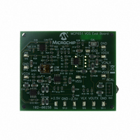
... Chapter 1. Product Overview 1.1 INTRODUCTION The MCP651 Input Offset Evaluation Board is described by the following: • Assembly # : 102-00258-R2 • Order # : MCP651EV-VOS • Name: MCP651 Input Offset Evaluation Board Items discussed in this chapter include: • Kit Contents • Intended Use • Description 1.2 KIT CONTENTS • ...
Page 10
... MCP651’s typical DDX SSX = 6 mA): Q Ω ≈ DDX DDI Q DDI ( Ω ) ≈ – SSX SSI Q SSI ) OST ) plus changes due to and 1/f noise which Evaluation Board Bias Voltage ( CMX V DDI V SSI V OUTX CALX + 60 mV – © 2009 Microchip Technology Inc. ...
Page 11
... U3, R11, R12, C6 “Integrator (ω U3, R17, C7 U4, R23, R24, R25, R26, S2 R28, C12 “Lowpass Filter (ω Note 1: Switch S2’s top position is closed when to the right (LOW GAIN), and is open when to the left (HI GAIN). © 2009 Microchip Technology Inc. OST CMX R 3 +2.5V ...
Page 12
... A M has a noise power bandwidth (NPBW) set by M ≈ 1.6 Hz) reduces this 1/f noise a little more before it is seen through R do not 5 8 input filters from COX connector COX = 5.6V (given OUTX ) is INT and COX and © 2009 Microchip Technology Inc. ...
Page 13
... V be, but doesn’t have to be, at mid-range set, as previously explained equal to V OUTX control loop railed at the corresponding supply voltage. The load resistor (R usually set to mid-supply. The V loading on V OUTX © 2009 Microchip Technology Inc. = 0V). CMX 4.49Ω 4.49Ω ...
Page 14
... DUT’s output voltage used only to verify that the circuit OUTX is the most important output resistors R and R ; this SSX closed by the user and that the MCP651 enters 9 (after SSX + 0.11s, which is slow 100 kΩ 1.0 µF 10 kΩ and V are DDI SSI multiplied by either OST © 2009 Microchip Technology Inc. ...
Page 15
... Lab Power Supplies - Drive V CALX in the next section) - Adjustable up to ±7.0V • Voltmeters - Measure resolution - -6V to +6V minimum range - Differential measurement (e.g., hand held meter) © 2009 Microchip Technology Inc. MCP651 INPUT OFFSET EVALUATION BOARD , GND, V (adjustable up to ±7.0V; optional if DDX SSX = -2.5V) SSX , V ...
Page 16
... Power Supply for VLX (Load Resistor’s bias point) a) Can be left open (fewer lab power supplies Can be shorted to GND with a jumper wire (VLX = 0V and R c) Can connect to an external lab power supply (R DS51834A-page 201 V/V 1998 V/V OST = 40 kΩ). kΩ). L © 2009 Microchip Technology Inc kΩ). L ...
Page 17
... For the best accuracy and ease of use, short VCALX to GND, set the other voltages for the desired bias during calibration, then initiate a calibration event in the DUT (push S1). Change the bias point afterwards to see how V OST © 2009 Microchip Technology Inc. at 0.3V below negative rail). CMX CALX = V = 0V) ...
Page 18
... This voltage is where the DUT’s common mode 43 CALX Conversion Equations (V) ← – V DDX DD CM ← – V SSX SS CM ← V – 1.3 0 – ← V – 0.2 V – V OUTX OUT CM ← – ← V – 1.4 V – V CALX CAL CM (Note 4) range vs OUT Result © 2009 Microchip Technology Inc. ...
Page 19
... V OS Example 2-1 gives an example of how V voltage ( EXAMPLE 2-1: Given 0.5 mV, OST V = 1.0 mV, OST Then: ΔV = 0.5 mV OST ΔV = 5.0V CM CMRR = 5. © 2009 Microchip Technology Inc. ) can be calculated from a measurement as OST ⁄ OST M A /Δ – ΔV )/Δ /Δ and changes in input offset as bias voltages and temperature change ...
Page 20
... Equation 2-1): Mk Estimates Units – (3.0V) µV/V OST_6 µV µV µV µV – (165°C) µV/°C OST_11 – (4.5V) µV/V OST_2 – (5.1V) µV/V OST_4 µV – (1.5V) µV/V OST_7 – (2.1V) µV/V OST_9 © 2009 Microchip Technology Inc. ...
Page 21
... Note: Sampling much faster than 10 SPS will not improve the averaged noise significantly. © 2009 Microchip Technology Inc. and noise voltage), between the DUT’s OST will appear to wander over time. The standard deviation of this ...
Page 22
... NOTES: DS51834A-page 18 © 2009 Microchip Technology Inc. ...
Page 23
... INTRODUCTION This chapter shows how to modify the MCP651 Input Offset Evaluation Board to measure other single op amps from Microchip Technology Inc. Items discussed in this chapter include: • Range of Parts Supported by the MCP651 Input Offset Evaluation Board • Changes to Accommodate Other DUTs 3 ...
Page 24
... There is a minimum Gain Bandwidth Product (GBWP) to keep the feedback loop stable, and a maximum GBWP to avoid crosstalk and other issues. EQUATION 3-3: DS51834A-page 20 and V values supported (relative ≤ V – ≤ V – ≤ ≤ 500 kHz GBWP 100 MHz ) are: CM © 2009 Microchip Technology Inc. ...
Page 25
... Since these boards come with the DUT (in SOIC-8) soldered on necessary to de-solder them. Figure 3-2 shows the location of the DUT for either a SOIC PDIP-8 package. A good de-soldering station makes this work much easier to do. FIGURE 3-2: © 2009 Microchip Technology Inc. and CAL/CS). The MCP651 Input Offset Evaluation CAL MCP651 ...
Page 26
... The adaptor boards approach may not work well in two cases: • Fast op amps (i.e., GBWP > 10 MHz); adding bypass capacitors to the adaptor board may help • Accurate op amps (i.e., V DS51834A-page 22 PCB with SOIC-8 Part Removed and DIP-8 IC Socket Installed. < ±50 µV) OST < ±50 µV) OST © 2009 Microchip Technology Inc. ...
Page 27
... Figure 3-4 shows a SOIC-8 op amp soldered onto the 8-Pin SOIC/MSOP/TSSOP/DIP Evaluation Board available from Microchip Technology Inc. The two interconnect strips on the bottom are soldered into the through holes for the DIP-8 socket. Figure 3-5 shows this board plugged into the MCP651 Input Offset Evaluation Board. ...
Page 28
... NOTES: DS51834A-page 24 © 2009 Microchip Technology Inc. ...
Page 29
... R through R 21 • R and The Gerber files for this board are available on the Microchip website (www.microchip.com) and are contained in the zip file “00258R2_Gerbers.zip”. © 2009 Microchip Technology Inc. MCP651 INPUT OFFSET EVALUATION BOARD 4 23 USER’S GUIDE DS51834A-page 25 ...
Page 30
... A.3 BOARD – SCHEMATIC DS51834A-page 26 © 2009 Microchip Technology Inc. ...
Page 31
... A.4 BOARD – COMBINATION OF THE TOP SILK-SCREEN, TOP SOLDER MASK AND TOP METAL LAYERS © 2009 Microchip Technology Inc. DS51834A-page 27 ...
Page 32
... A.5 BOARD – TOP SILK-SCREEN DS51834A-page 28 © 2009 Microchip Technology Inc. ...
Page 33
... A.6 BOARD – TOP SOLDER MASK AND TOP METAL LAYER © 2009 Microchip Technology Inc. DS51834A-page 29 ...
Page 34
... A.7 BOARD – BOTTOM METAL LAYER DS51834A-page 30 © 2009 Microchip Technology Inc. ...
Page 35
... R29, R30 4.99Ω, 1206 SMD, 1%, 1/4W Note 1: The components listed in this Bill of Materials are representative of the PCB assembly. The released BOM used in manufacturing uses all RoHS-compliant components. © 2009 Microchip Technology Inc. MCP651 INPUT OFFSET EVALUATION BOARD Description Manufacturer Panasonic ...
Page 36
... Designator 0 C1 Unknown Value, 0603 SMD, X7R, 16V, 10% Note 1: The components listed in this Bill of Materials are representative of the PCB assembly. The released BOM used in manufacturing uses all RoHS-compliant components. © 2009 Microchip Technology Inc. Description Manufacturer Panasonic-ECG Panasonic-ECG Panasonic-ECG Bournes Inc. ...
Page 37
... SMD, X7R, 16V, 10% 1 — Single Op Amp in Standard 8-pin pinout Note 1: The components listed in this Bill of Materials are representative of the PCB assembly. The released BOM used in manufacturing uses all RoHS-compliant components. © 2009 Microchip Technology Inc. Description Manufacturer Microchip Technology Inc. Samtec Inc. Panasonic Microchip Technology Inc ...
Page 38
... Fax: 886-3-6578-370 Taiwan - Kaohsiung Tel: 886-7-536-4818 Fax: 886-7-536-4803 Taiwan - Taipei Tel: 886-2-2500-6610 Fax: 886-2-2508-0102 Thailand - Bangkok Tel: 66-2-694-1351 Fax: 66-2-694-1350 © 2009 Microchip Technology Inc. EUROPE Austria - Wels Tel: 43-7242-2244-39 Fax: 43-7242-2244-393 Denmark - Copenhagen Tel: 45-4450-2828 Fax: 45-4485-2829 France - Paris Tel: 33-1-69-53-63-20 ...