MCP651EV-VOS Microchip Technology, MCP651EV-VOS Datasheet - Page 23
MCP651EV-VOS
Manufacturer Part Number
MCP651EV-VOS
Description
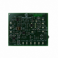
BOARD EVAL OP AMP MCP651
Manufacturer
Microchip Technology
Series
mCal Technologyr
Specifications of MCP651EV-VOS
Channels Per Ic
1 - Single
Amplifier Type
General Purpose
Output Type
Single-Ended, Rail-to-Rail
Slew Rate
30 V/µs
Current - Output / Channel
100mA
Operating Temperature
-40°C ~ 125°C
Current - Supply (main Ic)
6mA
Voltage - Supply, Single/dual (±)
2.5 V ~ 5.5 V
Board Type
Fully Populated
Utilized Ic / Part
MCP651
Processor To Be Evaluated
MCP651
Maximum Operating Temperature
+ 125 C
Minimum Operating Temperature
- 40 C
Operating Supply Voltage
2.5 V to 5.5 V
Tool Type
Evaluation Board
Core Architecture
PIC
Cpu Core
PIC
Data Bus Width
8 bit
Lead Free Status / RoHS Status
Lead free / RoHS Compliant
-3db Bandwidth
-
Lead Free Status / Rohs Status
Lead free / RoHS Compliant
Available stocks
Company
Part Number
Manufacturer
Quantity
Price
Company:

Part Number:
MCP651EV-VOS
Manufacturer:
Microchip Technology
Quantity:
135
Company:
Part Number:
MCP651EV-VOS
Manufacturer:
MICROCHIP
Quantity:
12 000


3.1
3.2
© 2009 Microchip Technology Inc.
INTRODUCTION
RANGE OF PARTS SUPPORTED BY MCP651 INPUT OFFSET EVALUATION
BOARD
This chapter shows how to modify the MCP651 Input Offset Evaluation Board to
measure other single op amps from Microchip Technology Inc. Items discussed in this
chapter include:
• Range of Parts Supported by the MCP651 Input Offset Evaluation Board
• Changes to Accommodate Other DUTs
Only op amps that fall within a certain performance range are supported by the
MCP651 Input Offset Evaluation Board.
3.2.1
In order to keep op amps U3 and U4 operating normally, the DUT’s V
EQUATION 3-1:
More accurate op amps need higher gain for good resolution. Table 3-1 shows what
V
TABLE 3-1:
Note 1:
OS
Where:
Chapter 3. Possible Modifications
specs can be supported for different voltmeter resolutions and amplifier gains.
High Gain = 1998 V/V
Low Gain = 201 V/V
2:
Voltmeter Resolution
These results assume a minimum measurement resolution of 1% of the V
The DUT needs to be soldered to the PCB when the maximum V
±50 µV, or so. Inserting a PDIP-8 part into a 8-pin socket creates a contact potential
(error) of the order of ±1 µV. Also, 1/f noise needs to be low.
Input Offset Voltage
0.1 mV
LOWER LIMIT ON V
1 mV
(mV)
V
V
OS
OS
<
<
±
±
12.4 mV, Low Gain
1.25 mV, High Gain
OS
MCP651 INPUT OFFSET
RANGE (NOTE 1)
EVALUATION BOARD
1998 (high gain)
1998 (high gain)
201 (low gain)
201 (low gain)
G
(V/V)
A
G
M
USER’S GUIDE
OST
OS
DS51834A-page 19
max(V
5 (Note 2)
must be:
(±µV)
is less than
500
50
50
OS
OS
) ≥
range.
Related parts for MCP651EV-VOS
Image
Part Number
Description
Manufacturer
Datasheet
Request
R

Part Number:
Description:
Manufacturer:
Microchip Technology Inc.
Datasheet:
Part Number:
Description:
Manufacturer:
Microchip Technology Inc.
Datasheet:
Part Number:
Description:
Manufacturer:
Microchip Technology Inc.
Datasheet:
Part Number:
Description:
Manufacturer:
Microchip Technology Inc.
Datasheet:
Part Number:
Description:
Manufacturer:
Microchip Technology Inc.
Datasheet:
Part Number:
Description:
Manufacturer:
Microchip Technology Inc.
Datasheet:
Part Number:
Description:
Manufacturer:
Microchip Technology Inc.
Datasheet:
Part Number:
Description:
Manufacturer:
Microchip Technology Inc.
Datasheet: