MCP651EV-VOS Microchip Technology, MCP651EV-VOS Datasheet - Page 3
MCP651EV-VOS
Manufacturer Part Number
MCP651EV-VOS
Description
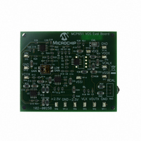
BOARD EVAL OP AMP MCP651
Manufacturer
Microchip Technology
Series
mCal Technologyr
Specifications of MCP651EV-VOS
Channels Per Ic
1 - Single
Amplifier Type
General Purpose
Output Type
Single-Ended, Rail-to-Rail
Slew Rate
30 V/µs
Current - Output / Channel
100mA
Operating Temperature
-40°C ~ 125°C
Current - Supply (main Ic)
6mA
Voltage - Supply, Single/dual (±)
2.5 V ~ 5.5 V
Board Type
Fully Populated
Utilized Ic / Part
MCP651
Processor To Be Evaluated
MCP651
Maximum Operating Temperature
+ 125 C
Minimum Operating Temperature
- 40 C
Operating Supply Voltage
2.5 V to 5.5 V
Tool Type
Evaluation Board
Core Architecture
PIC
Cpu Core
PIC
Data Bus Width
8 bit
Lead Free Status / RoHS Status
Lead free / RoHS Compliant
-3db Bandwidth
-
Lead Free Status / Rohs Status
Lead free / RoHS Compliant
Available stocks
Company
Part Number
Manufacturer
Quantity
Price
Company:

Part Number:
MCP651EV-VOS
Manufacturer:
Microchip Technology
Quantity:
135
Company:
Part Number:
MCP651EV-VOS
Manufacturer:
MICROCHIP
Quantity:
12 000


Preface ........................................................................................................................... 1
Chapter 1. Product Overview
Chapter 2. Installation and Operation
Chapter 3. Possible Modifications
Appendix A. Schematics and Layouts
© 2009 Microchip Technology Inc.
Introduction............................................................................................................ 1
Document Layout .................................................................................................. 1
Conventions Used in this Guide ............................................................................ 2
Recommended Reading........................................................................................ 3
The Microchip Web Site ........................................................................................ 3
Customer Support ................................................................................................. 3
Document Revision History ................................................................................... 4
1.1 Introduction ..................................................................................................... 5
1.2 Kit Contents .................................................................................................... 5
1.3 Intended Use .................................................................................................. 6
1.4 Description ..................................................................................................... 6
2.1 Introduction ................................................................................................... 11
2.2 Required Tools ............................................................................................. 11
2.3 Configuring the Lab Equipment and PCB .................................................... 12
2.4 Operating Conditions .................................................................................... 14
2.5 Converting to Other Parameters .................................................................. 15
2.6 Settling Time, Noise and Sampling Rate ...................................................... 17
3.1 Introduction ................................................................................................... 19
3.2 Range of Parts Supported by MCP651 Input Offset Evaluation Board ........ 19
3.3 Changes to Accommodate Other DUTs ....................................................... 21
A.1 Introduction .................................................................................................. 25
A.2 Schematic and Layouts ................................................................................ 25
A.3 Board – Schematic ....................................................................................... 26
A.4 Board – Combination of the Top Silk Screen, Top Solder Mask and Top Metal
A.5 Board – Top Silk Screen .............................................................................. 28
A.6 Board – Top Solder Mask and Top Metal Layer .......................................... 29
A.7 Board – Bottom Metal Layer ........................................................................ 30
Layers ..................................................................................................... 27
Table of Contents
MCP651 INPUT OFFSET
EVALUATION BOARD
USER’S GUIDE
DS51834A-page iii
Related parts for MCP651EV-VOS
Image
Part Number
Description
Manufacturer
Datasheet
Request
R

Part Number:
Description:
Manufacturer:
Microchip Technology Inc.
Datasheet:
Part Number:
Description:
Manufacturer:
Microchip Technology Inc.
Datasheet:
Part Number:
Description:
Manufacturer:
Microchip Technology Inc.
Datasheet:
Part Number:
Description:
Manufacturer:
Microchip Technology Inc.
Datasheet:
Part Number:
Description:
Manufacturer:
Microchip Technology Inc.
Datasheet:
Part Number:
Description:
Manufacturer:
Microchip Technology Inc.
Datasheet:
Part Number:
Description:
Manufacturer:
Microchip Technology Inc.
Datasheet:
Part Number:
Description:
Manufacturer:
Microchip Technology Inc.
Datasheet: