HW-SD1800A-DSP-SB-UNI-G Xilinx Inc, HW-SD1800A-DSP-SB-UNI-G Datasheet - Page 9
HW-SD1800A-DSP-SB-UNI-G
Manufacturer Part Number
HW-SD1800A-DSP-SB-UNI-G
Description
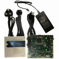
KIT DEVELOPMENT SPARTAN 3ADSP
Manufacturer
Xilinx Inc
Series
Spartan™-3A DSPr
Type
DSPr
Datasheet
1.HW-SD1800A-DSP-SB-UNI-G.pdf
(38 pages)
Specifications of HW-SD1800A-DSP-SB-UNI-G
Contents
Development Platform, Power Supply and software
Silicon Manufacturer
Xilinx
Features
10/100/1000 PHY, JTAG Programming And Configuration Port
Silicon Family Name
Spartan-3A
Silicon Core Number
3SD1800A-FG676
Lead Free Status / RoHS Status
Lead free / RoHS Compliant
For Use With/related Products
Spartan 3A
Lead Free Status / RoHS Status
Lead free / RoHS Compliant, Lead free / RoHS Compliant
Other names
122-1574
HW-SD1800A-DSP-DB-UNI-G
HW-SD1800A-DSP-DB-UNI-G
HW-SD1800A-DSP-SB-UNI-G
HW-SD1800A-DSP-DB-UNI-G
HW-SD1800A-DSP-DB-UNI-G
HW-SD1800A-DSP-SB-UNI-G
Available stocks
Company
Part Number
Manufacturer
Quantity
Price


Spartan-3A DSP Starter Platform User Guide
UG454 (v1.1) January 30, 2009
Memory
R
Micron DDR2 SDRAM Interface
Table 2: XC3SD1800A Input and Output Allocation (Cont’d)
The Spartan-3A DSP Starter Platform is populated with both high-speed RAM (128Mbytes
DDR2) and non-volatile ROM (16Mbytes parallel, and 64Mbit serial) to support various
types of applications. Additionally, a 50-pin connector is provided for SystemACE
interface (not included) that can be used to configure the Spartan-3A DSP FPGA, and to
provide storage for A/V media files from removable Compact Flash cards.
a high-level block diagram of the memory interfaces on this board.
X-Ref Target - Figure 2
Two Micron MT47H32M16BM DDR2 devices provide 128Mbytes of 32-bit wide memory
to the FPGA. The FPGA DDR2 interface supports SSTL18 signaling and all DDR2 signals
are controlled impedance. The DDR2 data, mask, and strobe signals are matched length
across all signals. Using I/O Bank 3 the DDR2 pinout on the FPGA is MIG-compliant.
Pinout of the FPGA DDR2 interface is provided in
SSTL18 Class I termination (series termination at the driving node and stub termination at
the receiving node) is used between the FPGA and DDR on all unidirectional signals, such
as Address, Control, and Clock. SSTL18 Class II termination (series and stub termination
at both nodes) is used on the FPGA side of the interface for all bidirectional signals such as
Data and Strobe. No board terminations are implemented for Data and Strobe on the
memory side. ODT is strapped as enabled, although an FPGA I/O is still connected to
allow the FPGA to drive this off. Note that stub terminations for address and control
signals are not populated in production based on HyperLynx simulation and exhaustive,
error-free testing of the FPGA-DDR2 interface at 133MHz.
Note:
1. FLASH_DO and SPI_MISO are a common pin.
I/O Bank
Number
3
3
System ACE
Connector
DDR2 Memory
I/O Function
Figure 2: Spartan-3A DSP Memory Interface
Ethernet
www.xilinx.com
Spartan
3A DSP
FPGA
Number
of I/O
Pins
73
17
Table 3
Number of
Input-only
Pins
13
0
32
8
1
below.
Translation
DDR2 SDRAM
Voltage
Parallel Flash
Functional Description
Serial Flash
2.5 V
(128 MB)
(64 Mbit)
(16 MB)
UG454_02_050908
Figure 2
Bank I/O
Voltage
1.8 V
shows
33
Related parts for HW-SD1800A-DSP-SB-UNI-G
Image
Part Number
Description
Manufacturer
Datasheet
Request
R

Part Number:
Description:
KIT DEVELOPMENT SPARTAN 3ADSP
Manufacturer:
Xilinx Inc

Part Number:
Description:
IC CPLD .8K 36MCELL 44-VQFP
Manufacturer:
Xilinx Inc
Datasheet:

Part Number:
Description:
IC CPLD 72MCRCELL 10NS 44VQFP
Manufacturer:
Xilinx Inc
Datasheet:

Part Number:
Description:
IC CPLD 1.6K 72MCELL 64-VQFP
Manufacturer:
Xilinx Inc
Datasheet:

Part Number:
Description:
IC CR-II CPLD 64MCELL 44-VQFP
Manufacturer:
Xilinx Inc
Datasheet:

Part Number:
Description:
IC CPLD 1.6K 72MCELL 100-TQFP
Manufacturer:
Xilinx Inc
Datasheet:

Part Number:
Description:
IC CR-II CPLD 64MCELL 56-BGA
Manufacturer:
Xilinx Inc
Datasheet:

Part Number:
Description:
IC CPLD 72MCRCELL 7.5NS 44VQFP
Manufacturer:
Xilinx Inc
Datasheet:
Part Number:
Description:
IC CR-II CPLD 64MCELL 100-VQFP
Manufacturer:
Xilinx Inc
Datasheet:
Part Number:
Description:
IC CPLD 1.6K 72MCELL 100-TQFP
Manufacturer:
Xilinx Inc
Datasheet:

Part Number:
Description:
IC CPLD 72MCRCELL 7.5NS 64VQFP
Manufacturer:
Xilinx Inc
Datasheet:
Part Number:
Description:
IC CPLD 1.6K 72MCELL 100-TQFP
Manufacturer:
Xilinx Inc
Datasheet:

Part Number:
Description:
IC CPLD 1.5K 64MCELL HP 44-VQFP
Manufacturer:
Xilinx Inc

Part Number:
Description:
IC CPLD 36MCRCELL 15NS 44PLCC
Manufacturer:
Xilinx Inc
Datasheet:

Part Number:
Description:
IC CPLD 36MCRCELL 10NS 44PLCC
Manufacturer:
Xilinx Inc
Datasheet: