CY3684 Cypress Semiconductor Corp, CY3684 Datasheet - Page 14
CY3684
Manufacturer Part Number
CY3684
Description
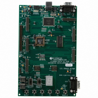
KIT DEVELOPMENT EZ-USB FX2LP
Manufacturer
Cypress Semiconductor Corp
Series
EZ-USB FXr
Type
MCUr
Datasheet
1.CY3684.pdf
(28 pages)
Specifications of CY3684
Contents
2 Boards, Cables, CD
Silicon Manufacturer
Cypress
Application Sub Type
USB
Kit Application Type
Interface
Silicon Core Number
CY7C68013A-128AXC
Features
FX2LP Development Kit
Silicon Family Name
EZ-USB FX2LP
Rohs Compliant
No
Lead Free Status / RoHS Status
Contains lead / RoHS non-compliant
For Use With/related Products
CY7C68013A-128AC, CY7C64713-128AC
Lead Free Status / RoHS Status
Contains lead / RoHS non-compliant
Other names
428-1677
CY3684
Q2204408
CY3684
Q2204408


Because the 20-pin headers on the proto-typing board are stackable, it is possible to build custom
circuitry on the proto board, plug the board into the EZ-USB Development board, and still plug
logic analyzer pods into the six connectors P1-P6.
Tables 4-9 show the EZ-USB pin designations for P1 through P6. For dual-mode pins, the power-
on default signal names are shown in bold type, and the alternate pin names are shown in the out-
side columns.
Page -10
•
•
•
High speed EZ-USB strobe signals (PSEN, WR#, CLKOUT, IFCLK, and RD#) are con-
nected to pin 3 of each of the five connectors P1-P6, so that they may be used as the logic
analyzer clock CLK1.
CLK2 is not used. Instead, each connector brings 3.3V power from the EZ-USB Develop-
ment Board up to the prototype board using pin 2.
The signals are logically grouped. For example, the 8051 address bus is on P5, and the
EZ-USB FIFO data (which shares PORTB and PORTD pins) is on P1.
Alternate
Alternate
FIFOADR0
PKTEND
FD[14]
FD[12]
FD[10]
FLAGC
FLAGA
FD[8]
FD[6]
FD[4]
FD[2]
FD[0]
SLRD
SLOE
INT0#
Default
Default
PSEN#
RDY0
CTL4
CTL2
CTL0
N.C.
PD6
PD4
PD2
PD0
PB6
PB4
PB2
PB0
N.C.
N.C.
PA6
PA4
PA2
PA0
Table 4.
Table 5.
11
13
15
17
19
1
3
5
7
9
11
13
15
17
19
1
3
5
7
9
P1
P2
EZ-USB Development Kit Manual - Getting Started Rev 1.0
12
10
14
16
18
20
2
4
6
8
10
12
14
16
18
20
2
4
6
8
3.3V
PD7
PD5
PD3
PD1
PB7
PB5
PB3
PB1
GND
3.3V
RDY1
CTL5
CTL3
CTL1
PA7
PA5
PA3
PA1
GND
Default
Default
FD[15]
FD[13]
FD[11]
FD[9]
FD[7]
FD[5]
FD[3]
FD[1]
SLWR
FLAGB
FLAGD
FIFOADR1
WU2
INT1#
Alternate
Alternate
Related parts for CY3684
Image
Part Number
Description
Manufacturer
Datasheet
Request
R

Part Number:
Description:
Manufacturer:
Cypress Semiconductor Corp
Datasheet:
Part Number:
Description:
Manufacturer:
Cypress Semiconductor Corp
Datasheet:
Part Number:
Description:
Manufacturer:
Cypress Semiconductor Corp
Datasheet:
Part Number:
Description:
Manufacturer:
Cypress Semiconductor Corp
Datasheet:
Part Number:
Description:
Manufacturer:
Cypress Semiconductor Corp
Datasheet: