DEMO9S08LL16 Freescale Semiconductor, DEMO9S08LL16 Datasheet
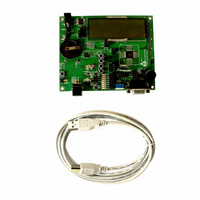
DEMO9S08LL16
Specifications of DEMO9S08LL16
Available stocks


Related parts for DEMO9S08LL16

DEMO9S08LL16 Summary of contents
Page 1
... Freescale Semiconductor Data Sheet: Technical Data An Energy Efficient Solution by Freescale MC9S08LL16 Series Covers: MC9S08LL16 and MC9S08LL8 Features • 8-Bit HCS08 Central Processor Unit (CPU) – 20-MHz CPU at 3.6V to 1.8V across temperature range of -40°C to 85°C – HC08 instruction set with added BGND instruction – ...
Page 2
... PU PD Figure PTA[4:5], PTD[0:77] and PTE[0: MC9S08LL16 Series MCU Data Sheet, Rev. 6 Figure , DDAD DDA Completed the Figure in the InT at 8 MHz, FEI mode with all DD in the Table and E in the Table 18. IL Freescale Semiconductor 3. in the k ...
Page 3
... Related Documentation Find the most current versions of all documents at: http://www.freescale.com Reference Manual (MC9S08LL16RM) Contains extensive product information including modes of operation, memory, resets and interrupts, register definition, port pins, CPU, and all module information. Freescale Semiconductor MC9S08LL16 Series MCU Data Sheet, Rev ...
Page 4
... Yes Yes 8x24 8x16 4x28 4x20 shows the structure of the MC9S08LL16 series MCU. MC9S08LL16 Series MCU Data Sheet, Rev. 6 MC9S08LL8 48-pin QFN/LQFP 10,240 (8K and 2K arrays) 2080 yes 8-ch yes yes 8 yes yes 2-ch - Yes 8x16 4x20 31 Freescale Semiconductor ...
Page 5
... V DD VOLTAGE REGULATOR DDA REFH V /V SSA REFL Figure 1. MC9S08LL16 Series Block Diagram Freescale Semiconductor ON-CHIP ICE DEBUG MODULE (DBG) TIME OF DAY MODULE (TOD) 8-BIT KEYBOARD INTERRUPT (KBI) BKGD/MS SERIAL PERIPHERAL INTERFACE (SPI) RESET IRQ IIC MODULE (IIC) 2-CHANNEL TIMER/PWM (TPM2) ...
Page 6
... Note are internally connected to V REFH REFL Figure 2. MC9S08LL16 Series in 64-pin LQFP Package 64-Pin LQFP DDA SSA MC9S08LL16 Series MCU Data Sheet, Rev. 6 LCD26 48 LCD27 47 LCD28 46 LCD29 45 PTA5/KBIP5/ADP5/LCD30 44 PTA4/KBIP4/ADP4/LCD31 43 PTA3/KBIP3/SCL/MOSI/ADP3 42 PTA2/KBIP2/SDA/MISO/ADP2 41 PTA1/KBIP1/SPSCK/ADP1 40 PTA0/KBIP0/SS/ADP0 39 PTC7/IRQ/TCLK 38 PTC6/ACMPO/BKGD/MS 37 PTC5/TPM2CH1 36 PTC4/TPM2CH0 35 PTC3/TPM1CH1 34 PTC2/TPM1CH0 33 Freescale Semiconductor ...
Page 7
... PTD4/LCD4/ 5 PTD3/LCD3 6 PTD2/LCD2 7 PTD1/LCD1 8 PTD0/LCD0 9 V CAP1 10 V CAP2 11 V LL1 12 V LL2 14 13 Note: V REFH Figure 3. MC9S08LL16 Series in 48-Pin QFN/LQFP Packages Freescale Semiconductor 48-Pin QFN/LQFP are internally connected to V REFL MC9S08LL16 Series MCU Data Sheet, Rev. 6 Pin Assignments 37 36 LCD28 ...
Page 8
... MISO — MOSI — SPSCK — SS RxD TxD TPM1CH0 TPM1CH1 TPM2CH0 TPM2CH1 ACMPO BKGD IRQ KBIP0 — MC9S08LL16 Series MCU Data Sheet, Rev. 6 --> Highest Alt3 Alt4 ACMP+ ACMP– V SSA V REFL V REFH V DDA SDA SCL MS TCLK SS ADP0 Freescale Semiconductor ...
Page 9
... Parameter Classification The electrical parameters shown in this supplement are guaranteed by various methods. To give the customer a better understanding the following classification is used and the parameters are tagged accordingly in the tables where appropriate: Freescale Semiconductor <-- Lowest Priority Alt 1 Alt 2 KBIP1 — ...
Page 10
... DD MC9S08LL16 Series MCU Data Sheet, Rev the programmable SS DD Value Unit –0.3 to 3.8 V 120 mA –0 0 C –55 to 150 ) and negative (V ) clamp DD SS and range during instantaneous and > greater than In DD Freescale Semiconductor ...
Page 11
... Watts — chip internal power int Power dissipation on input and output pins — user determined I/O P For most applications, P I/O ( neglected) is: I/O Solving Equation 3-1 and Equation 3-2 Freescale Semiconductor Table 5. Thermal Characteristics Symbol JA C can be obtained from: J ...
Page 12
... Symbol R1 C — — 1 Symbol Rating V HBM V CDM = 85 LAT MC9S08LL16 Series MCU Data Sheet, Rev. 6 and T can be obtained Value Unit 1500 100 pF 3 0 200 pF 3 –2.5 V 7.5 V Min Max Unit 2000 — V 500 — V 100 — mA Freescale Semiconductor ...
Page 13
... C Output low 7 D Max total I current P Input high 8 voltage C P Input low 9 voltage C Input 10 C hysteresis Input leakage all input only pins 11 P current Freescale Semiconductor Table 8. DC Characteristics Symbol Condition V >1 –0.6 mA Load V V > 2 –10 mA Load > 1.8 V ...
Page 14
... V falling 1.80 1.84 1. rising 1.88 1.92 1. falling DD 2.08 2.14 V rising DD — 80 1.15 1.17 1.18 and load will shunt current greater than maximum DD Freescale Semiconductor Unit A 1 A 2 k 0 1.0 V 2.0 V s — V 2.2 V — and could DD ...
Page 15
... Figure 4. Non-LCD pins I/O Pullup and Pulldown Typical Resistor Values (V Freescale Semiconductor MC9S08LL16 Series MCU Data Sheet, Rev. 6 Electrical Characteristics = 3 ...
Page 16
... Electrical Characteristics Figure 5. LCD/GPIO Pins I/O Pullup/Pulldown Typical Resistor Values 16 MC9S08LL16 Series MCU Data Sheet, Rev. 6 Freescale Semiconductor ...
Page 17
... Figure 6. Typical Low-Side Driver (Sink) Characteristics (Non-LCD pins) Freescale Semiconductor MC9S08LL16 Series MCU Data Sheet, Rev. 6 Electrical Characteristics Low Drive (PTxDSn = 0) — 17 ...
Page 18
... Electrical Characteristics Figure 7. Typical Low-Side Driver (Sink) Characteristics(Non-LCD pins) 18 MC9S08LL16 Series MCU Data Sheet, Rev. 6 High Drive (PTxDSn = 1) — Freescale Semiconductor ...
Page 19
... Figure 8. Typical High-Side (Source) Characteristics (Non-LCD Pins) Freescale Semiconductor MC9S08LL16 Series MCU Data Sheet, Rev. 6 Electrical Characteristics Low Drive (PTxDSn = 0) — 19 ...
Page 20
... Electrical Characteristics Figure 9. Typical High-Side (Source) Characteristics(Non-LCD Pins) 20 MC9S08LL16 Series MCU Data Sheet, Rev. 6 High Drive (PTxDSn = 1) — Freescale Semiconductor ...
Page 21
... I (mA) OL Figure 10. Typical Low-Side Driver (Sink) Characteristics (LCD/GPIO Pins) Freescale Semiconductor MC9S08LL16 Series MCU Data Sheet, Rev. 6 Electrical Characteristics Preliminary Low Drive (PTxDSn = 0) — 21 ...
Page 22
... Electrical Characteristics Figure 11. Typical Low-Side Driver (Sink) Characteristics(LCD/GPIO Pins) 22 MC9S08LL16 Series MCU Data Sheet, Rev. 6 High Drive (PTxDSn = 1) — Freescale Semiconductor ...
Page 23
... Figure 12. Typical High-Side (Source) Characteristics (LCD/GPIO Pins) Freescale Semiconductor MC9S08LL16 Series MCU Data Sheet, Rev. 6 Electrical Characteristics Low Drive (PTxDSn = 0) — 23 ...
Page 24
... Electrical Characteristics Figure 13. Typical High-Side (Source) Characteristics(LCD/GPIO pins) 24 MC9S08LL16 Series MCU Data Sheet, Rev. 6 High Drive (PTxDSn = 1) — Freescale Semiconductor ...
Page 25
... FEI mode, all modules off C Wait mode supply current 7 T LPRS = 1, all modules off P 8 Stop2 mode supply current C P Stop3 mode supply current 9 No clocks active C Freescale Semiconductor Table 9. Supply Current Characteristics V Bus Symbol Freq 8 MHz MHz 10 MHz MHz 16 kHz ...
Page 26
... Unit Typ (V) A 3 6.1 — A 3 7.5 — Temperature (C) – 100 100 150 175 250 360 400 460 100 110 110 112 115 101 120 1 1 4.2 12 Freescale Semiconductor Temp (C) 25 C 50 C Units nA nA A nA A A A A ...
Page 27
... Data in Typical column was characterized at 3.0 V, 25 typical recommended value. 2 Load capacitors ( ), feedback resistor ( See crystal or resonator manufacturer’s recommendation. 4 Proper PC board layout procedures must be followed to achieve specifications. Freescale Semiconductor for crystal or resonator circuits. Characteristic and series resistor ( ) are incorporated internally when RANGE=HGO= MC9S08LL16 Series MCU Data Sheet, Rev. 6 ...
Page 28
... Max f — 32.768 — int_ft f 31.25 — 39.063 int_t t — — 6 IRST 12.8 16.8 21.33 dco_ut f 16 — 20 dco_t 0.1 0.2 — 0.2 0.4 — + 0.5 2 — dco_t –1.0 Freescale Semiconductor Unit kHz kHz s MHz MHz %f dco %f dco %f dco ...
Page 29
... Measurements are made with the device powered by filtered supplies and clocked by a stable external clock signal. Noise injected into the FLL circuitry via V percentage for a given interval. Figure 16. Deviation of DCO Output from Trimmed Frequency (20 MHz, 3.0 V) Freescale Semiconductor Symbol ...
Page 30
... IHIL 1.5 t — — cyc t 100 — — IHIL 1.5 t — — cyc , t Fall — 16 — — 23 — Fall — 5 — — 9 — — MSH Freescale Semiconductor Unit MHz after V DD ...
Page 31
... External clock frequency 2 D External clock period 3 D External clock high time 4 D External clock low time 5 D Input capture pulse width TCLK Freescale Semiconductor t extrst Figure 17. Reset Timing t IHIL t ILIH Figure 18. IRQ/KBIPx Timing Table 14. TP Input Timing Function Symbol f TCLK ...
Page 32
... Max Unit f /2048 Bus Bus Bus 2 2048 t cyc 4 — t cyc 12 — t SPSCK 1 — t cyc 12 — t SPSCK 1 — t cyc t –30 1024 t ns cyc cyc t – 30 — ns cyc 15 — — — — ns — cyc — cyc — — Freescale Semiconductor ...
Page 33
... SPSCK (CPOL = 1) (OUTPUT MISO 2 MS BIN (INPUT) 9 MOSI 2 MSB OUT (OUTPUT) NOTES output mode (DDS7 = 1, SSOE = 1). 2. LSBF = 0. For LSBF = 1, bit order is LSB, bit 1, ..., bit 6, MSB. Freescale Semiconductor Table 15. SPI Timing (continued) Function Symbol BIT LSB IN 9 BIT LSB OUT Figure 21 ...
Page 34
... Not defined but normally MSB of character just received BIT BIT Figure 22. SPI Master Timing (CPHA = BIT BIT Figure 23. SPI Slave Timing (CPHA = 0) MC9S08LL16 Series MCU Data Sheet, Rev LSB IN MASTER LSB OUT PORT DATA SEE SLAVE LSB OUT NOTE 1 LSB IN Freescale Semiconductor ...
Page 35
... Analog input leakage current C Analog comparator initialization delay 3.12 ADC Characteristics Table 17. 12-bit ADC Operating Conditions Characteristic Conditions Absolute Supply voltage Delta Ground voltage Delta Freescale Semiconductor BIT MSB OUT 6 BIT Figure 24. SPI Slave Timing (CPHA = 1) Symbol Min V 1 DDAC V V AIN ...
Page 36
... MC9S08LL16 Series MCU Data Sheet, Rev Max Unit Comment V V DDA DDA — REFH 4.5 5 k — 2 — 5 k External to MCU — 5 — 10 — 10 — 8.0 MHz — 4.0 Z ADIN SIMPLIFIED CHANNEL SELECT CIRCUIT ADC SAR ENGINE R ADIN R ADIN R ADIN R ADIN C ADIN Freescale Semiconductor ...
Page 37
... Unadjusted 2.7>VDDA>1.8V Error P 10-bit mode T 8-bit mode T 12-bit mode Differential P Non-Linearity 10-bit mode T 8-bit mode T 12-bit mode Integral P Non-Linearity 10-bit mode T 8-bit mode Freescale Semiconductor REFH Symb Min I — DDA I — DDA I — DDA I — DDA 2 f ADACK 1.25 — t ADC — ...
Page 38
... LSB V ADIN 0.5 0.5 –3.5 to 1 1.0 2 LSB V 0.5 1 ADIN 0.5 0.5 – — 0.5 2 — LSB 0.5 — 2 — Pad leakage 0.2 4 2 LSB 0.1 1.2 1.646 — mV/C 1.769 — 701.2 — mV Freescale Semiconductor = V SSA = V DDA ...
Page 39
... This section provides details about program/erase times and program-erase endurance for the flash memory. Program and erase operations do not require any special power sources other than the normal V For more detailed information about program/erase operations, see the Memory section. Freescale Semiconductor Table 19. LCD Electricals Glass Symbol V ...
Page 40
... These values are measured at room temperatures DD MC9S08LL16 Series MCU Data Sheet, Rev. 6 Typical Max 3.6 3.6 200 5 6. 4000 20,000 4 — 6 — — — 100,000 — 100 — Freescale Semiconductor Unit V V kHz s t Fcyc t Fcyc t Fcyc t Fcyc mA mA cycles years ...
Page 41
... MC9S08LL16 Series Product Summary pages at http://www.freescale.com. To view the latest drawing, either: • Click on the appropriate link in • Open a browser to the Freescale document number (from Freescale Semiconductor Table 21. Radiated Emissions, Electric Field Conditions Frequency V = 3.3 V 0.15 – 50 MHz DD ...
Page 42
... Package Information and Mechanical Drawings Pin Count Package Type 64 Low Quad Flat Package 48 Low Quad Flat Package 48 Quad Flat No-Leads 42 Table 22. Package Descriptions Abbreviation Designator LQFP LQFP QFN MC9S08LL16 Series MCU Data Sheet, Rev. 6 Case No. Document No. LH 840F 98ASS23234W LF 932 98ASH00962A GT 1314 98ARH99048A Freescale Semiconductor ...
Page 43
... Freescale Semiconductor Package Information and Mechanical Drawings MC9S08LL16 Series MCU Data Sheet, Rev ...
Page 44
... Freescale Semiconductor was negligent regarding the design or manufacture of the part. Freescale™ and the Freescale logo are trademarks of Freescale Semiconductor, Inc ...