DEMO9S08LL16 Freescale Semiconductor, DEMO9S08LL16 Datasheet - Page 30
DEMO9S08LL16
Manufacturer Part Number
DEMO9S08LL16
Description
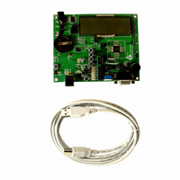
BOARD DEMO FOR MC9S08LL16 MCU
Manufacturer
Freescale Semiconductor
Series
HCS08r
Type
MCUr
Datasheets
1.DEMO9S08LL16.pdf
(44 pages)
2.DEMO9S08LL16.pdf
(15 pages)
3.DEMO9S08LL16.pdf
(8 pages)
4.DEMO9S08LL16.pdf
(2 pages)
Specifications of DEMO9S08LL16
Contents
Board, Cable, DVD
Silicon Manufacturer
Freescale
Core Architecture
HCS08
Core Sub-architecture
HCS08
Silicon Core Number
MC9S08
Silicon Family Name
S08LL
Kit Contents
Board
Rohs Compliant
Yes
For Use With/related Products
MC9S08LL16
Lead Free Status / RoHS Status
Contains lead / RoHS non-compliant
Available stocks
Company
Part Number
Manufacturer
Quantity
Price
Company:

Part Number:
DEMO9S08LL16
Manufacturer:
ALL
Quantity:
80


Electrical Characteristics
3.10
This section describes timing characteristics for each peripheral system.
3.10.1
30
1
2
3
4
5
6
Num
Typical values are based on characterization data at V
This is the shortest pulse that is guaranteed to be recognized as a reset pin request.
To enter BDM mode following a POR, BKGD/MS should be held low during the power-up and for a hold time of t
rises above V
This is the minimum pulse width that is guaranteed to pass through the pin synchronization circuitry. Shorter pulses may or
may not be recognized. In stop mode, the synchronizer is bypassed so shorter pulses can be recognized.
Timing is shown with respect to 20% V
Except for LCD pins in Open Drain mode.
10
1
2
3
4
5
6
7
8
9
C
D
D
D
D
D
D
D
D
C
C
AC Characteristics
Control Timing
Bus frequency (t
Internal low power oscillator period
External reset pulse width
Reset low drive
BKGD/MS setup time after issuing background debug
force reset to enter user or BDM modes
BKGD/MS hold time after issuing background debug
force reset to enter user or BDM modes
IRQ pulse width
Keyboard interrupt pulse width
Port rise and fall time — Non-LCD Pins
Low output drive (PTxDS = 0) (load = 50 pF)
Port rise and fall time — Non-LCD Pins
High output drive (PTxDS = 1) (load = 50 pF)
Voltage Regulator Recovery time
LVD
Asynchronous path
Synchronous path
Asynchronous path
Synchronous path
Slew rate control disabled (PTxSE = 0)
Slew rate control enabled (PTxSE = 1)
Slew rate control enabled (PTxSE = 1)
Slew rate control disabled (PTxSE = 0)
.
cyc
= 1/f
4
4
2
2
Rating
MC9S08LL16 Series MCU Data Sheet, Rev. 6
Bus
2
DD
)
and 80% V
Table 13. Control Timing
DD
3
DD
levels. Temperature range –40 C to 85 C.
5, 6
= 3.0 V, 25 C unless otherwise stated.
5, 6
t
t
t
t
Symbol
ILIH,
ILIH,
Rise
Rise
t
t
t
MSSU
t
t
t
rstdrv
f
extrst
MSH
VRR
LPO
Bus
, t
, t
t
t
IHIL
IHIL
Fall
Fall
1.5 t
1.5 t
34 t
Min
700
100
500
100
100
100
dc
—
—
—
—
—
cyc
cyc
cyc
Typ
16
23
—
—
—
—
—
—
—
—
—
—
Freescale Semiconductor
5
9
6
1
1300
Max
10
10
—
—
—
—
—
—
—
—
—
—
—
—
MSH
after V
MHz
Unit
s
ns
ns
ns
s
ns
ns
ns
ns
us
DD
Related parts for DEMO9S08LL16
Image
Part Number
Description
Manufacturer
Datasheet
Request
R

Part Number:
Description:
Manufacturer:
Freescale Semiconductor, Inc
Datasheet:
Part Number:
Description:
Manufacturer:
Freescale Semiconductor, Inc
Datasheet:
Part Number:
Description:
Manufacturer:
Freescale Semiconductor, Inc
Datasheet:
Part Number:
Description:
Manufacturer:
Freescale Semiconductor, Inc
Datasheet:
Part Number:
Description:
Manufacturer:
Freescale Semiconductor, Inc
Datasheet:
Part Number:
Description:
Manufacturer:
Freescale Semiconductor, Inc
Datasheet:
Part Number:
Description:
Manufacturer:
Freescale Semiconductor, Inc
Datasheet:
Part Number:
Description:
Manufacturer:
Freescale Semiconductor, Inc
Datasheet:
Part Number:
Description:
Manufacturer:
Freescale Semiconductor, Inc
Datasheet:
Part Number:
Description:
Manufacturer:
Freescale Semiconductor, Inc
Datasheet:
Part Number:
Description:
Manufacturer:
Freescale Semiconductor, Inc
Datasheet:
Part Number:
Description:
Manufacturer:
Freescale Semiconductor, Inc
Datasheet:
Part Number:
Description:
Manufacturer:
Freescale Semiconductor, Inc
Datasheet:
Part Number:
Description:
Manufacturer:
Freescale Semiconductor, Inc
Datasheet:
Part Number:
Description:
Manufacturer:
Freescale Semiconductor, Inc
Datasheet: