C8051F996DK Silicon Laboratories Inc, C8051F996DK Datasheet - Page 27
C8051F996DK
Manufacturer Part Number
C8051F996DK
Description
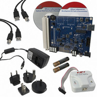
KIT DEV FOR C8051F996
Manufacturer
Silicon Laboratories Inc
Type
MCUr
Datasheets
1.C8051F996DK.pdf
(24 pages)
2.C8051F996DK.pdf
(2 pages)
3.C8051F996DK.pdf
(4 pages)
4.C8051F996DK.pdf
(322 pages)
Specifications of C8051F996DK
Contents
Board, Batteries, Cables, CDs, Debug Adapter, Documentation, Power Adapter
Processor To Be Evaluated
C8051F996
Processor Series
C8051F98x
Interface Type
USB
Operating Supply Voltage
3 V
Lead Free Status / RoHS Status
Lead free / RoHS Compliant
For Use With/related Products
C8051F996
Lead Free Status / Rohs Status
Lead free / RoHS Compliant
Other names
336-1963


1.3.
The C8051F99x-C8051F98x Family includes an SMBus/I
baud rate configuration, and an Enhanced SPI interface. Each of the serial buses is fully implemented in
hardware and makes extensive use of the CIP-51's interrupts, thus requiring very little CPU intervention.
1.4.
An on-chip programmable counter/timer array (PCA) is included in addition to the four 16-bit general
purpose counter/timers. The PCA consists of a dedicated 16-bit counter/timer time base with three
programmable capture/compare modules. The PCA clock is derived from one of seven sources: the
system clock divided by 12, the system clock divided by 4, Timer 0 overflows, an External Clock Input
(ECI), the system clock, the external oscillator clock source divided by 8, or the SmaRTClock divided by 8.
Each capture/compare module can be configured to operate in a variety of modes: edge-triggered capture,
software timer, high-speed output, pulse width modulator (8, 9, 10, 11, or 16-bit), or frequency output.
Additionally, Capture/Compare Module 2 offers watchdog timer (WDT) capabilities. Following a system
reset, Module 2is configured and enabled in WDT mode. The PCA Capture/Compare Module I/O and
External Clock Input may be routed to Port I/O via the Digital Crossbar.
Serial Ports
Programmable Counter Array
C a p tu r e /C o m p a r e
M o d u le 0
S Y S C L K / 1 2
S Y S C L K / 4
E x te r n a l C lo c k / 8
S m a R T C lo c k /8
Figure 1.15. PCA Block Diagram
T im e r 0 O v e rflo w
E C I
S Y S C L K
P o r t I/ O
C r o s s b a r
C a p tu re /C o m p a re
Rev. 1.0
C L O C K
M U X
M o d u le 1
P C A
C8051F99x-C8051F98x
2
C interface, a full-duplex UART with enhanced
1 6 -B it C o u n te r/ T im e r
C a p tu re / C o m p a re
M o d u le 2 / W D T
27
Related parts for C8051F996DK
Image
Part Number
Description
Manufacturer
Datasheet
Request
R

Part Number:
Description:
SMD/C°/SINGLE-ENDED OUTPUT SILICON OSCILLATOR
Manufacturer:
Silicon Laboratories Inc
Part Number:
Description:
Manufacturer:
Silicon Laboratories Inc
Datasheet:
Part Number:
Description:
N/A N/A/SI4010 AES KEYFOB DEMO WITH LCD RX
Manufacturer:
Silicon Laboratories Inc
Datasheet:
Part Number:
Description:
N/A N/A/SI4010 SIMPLIFIED KEY FOB DEMO WITH LED RX
Manufacturer:
Silicon Laboratories Inc
Datasheet:
Part Number:
Description:
N/A/-40 TO 85 OC/EZLINK MODULE; F930/4432 HIGH BAND (REV E/B1)
Manufacturer:
Silicon Laboratories Inc
Part Number:
Description:
EZLink Module; F930/4432 Low Band (rev e/B1)
Manufacturer:
Silicon Laboratories Inc
Part Number:
Description:
I°/4460 10 DBM RADIO TEST CARD 434 MHZ
Manufacturer:
Silicon Laboratories Inc
Part Number:
Description:
I°/4461 14 DBM RADIO TEST CARD 868 MHZ
Manufacturer:
Silicon Laboratories Inc
Part Number:
Description:
I°/4463 20 DBM RFSWITCH RADIO TEST CARD 460 MHZ
Manufacturer:
Silicon Laboratories Inc
Part Number:
Description:
I°/4463 20 DBM RADIO TEST CARD 868 MHZ
Manufacturer:
Silicon Laboratories Inc
Part Number:
Description:
I°/4463 27 DBM RADIO TEST CARD 868 MHZ
Manufacturer:
Silicon Laboratories Inc
Part Number:
Description:
I°/4463 SKYWORKS 30 DBM RADIO TEST CARD 915 MHZ
Manufacturer:
Silicon Laboratories Inc
Part Number:
Description:
N/A N/A/-40 TO 85 OC/4463 RFMD 30 DBM RADIO TEST CARD 915 MHZ
Manufacturer:
Silicon Laboratories Inc
Part Number:
Description:
I°/4463 20 DBM RADIO TEST CARD 169 MHZ
Manufacturer:
Silicon Laboratories Inc