C8051F996DK Silicon Laboratories Inc, C8051F996DK Datasheet - Page 9
C8051F996DK
Manufacturer Part Number
C8051F996DK
Description
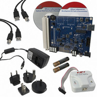
KIT DEV FOR C8051F996
Manufacturer
Silicon Laboratories Inc
Type
MCUr
Datasheets
1.C8051F996DK.pdf
(24 pages)
2.C8051F996DK.pdf
(2 pages)
3.C8051F996DK.pdf
(4 pages)
4.C8051F996DK.pdf
(322 pages)
Specifications of C8051F996DK
Contents
Board, Batteries, Cables, CDs, Debug Adapter, Documentation, Power Adapter
Processor To Be Evaluated
C8051F996
Processor Series
C8051F98x
Interface Type
USB
Operating Supply Voltage
3 V
Lead Free Status / RoHS Status
Lead free / RoHS Compliant
For Use With/related Products
C8051F996
Lead Free Status / Rohs Status
Lead free / RoHS Compliant
Other names
336-1963


Figure 7.3. CP0 Multiplexer Block Diagram.............................................................. 96
Figure 8.1. CS0 Block Diagram ................................................................................ 98
Figure 8.2. Auto-Scan Example.............................................................................. 101
Figure 8.3. CS0 Multiplexer Block Diagram............................................................ 116
Figure 9.1. CIP-51 Block Diagram.......................................................................... 118
Figure 10.1. C8051F99x-C8051F98x Memory Map ............................................... 127
Figure 10.2. Flash Program Memory Map.............................................................. 128
Figure 14.1. Flash Program Memory Map (8 kB and smaller devices) .................. 151
Figure 15.1. C8051F99x-C8051F98x Power Distribution....................................... 162
Figure 16.1. CRC0 Block Diagram ......................................................................... 170
Figure 16.2. Bit Reverse Register .......................................................................... 177
Figure 18.1. Reset Sources.................................................................................... 179
Figure 18.2. Power-Fail Reset Timing Diagram ..................................................... 180
Figure 19.1. Clocking Sources Block Diagram ....................................................... 186
Figure 19.2. 25 MHz External Crystal Example...................................................... 188
Figure 20.1. SmaRTClock Block Diagram.............................................................. 195
Figure 20.2. Interpreting Oscillation Robustness (Duty Cycle) Test Results.......... 204
Figure 21.1. Port I/O Functional Block Diagram ..................................................... 213
Figure 21.2. Port I/O Cell Block Diagram ............................................................... 214
Figure 21.3. Peripheral Availability on Port I/O Pins............................................... 217
Figure 21.4. Crossbar Priority Decoder in Example Configuration
Figure 21.5. Crossbar Priority Decoder in Example Configuration
Figure 22.1. SMBus Block Diagram ....................................................................... 233
Figure 22.2. Typical SMBus Configuration ............................................................. 234
Figure 22.3. SMBus Transaction ............................................................................ 235
Figure 22.4. Typical SMBus SCL Generation......................................................... 238
Figure 22.5. Typical Master Write Sequence ......................................................... 247
Figure 22.6. Typical Master Read Sequence ......................................................... 248
Figure 22.7. Typical Slave Write Sequence ........................................................... 249
Figure 22.8. Typical Slave Read Sequence ........................................................... 250
Figure 23.1. UART0 Block Diagram ....................................................................... 255
Figure 23.2. UART0 Baud Rate Logic .................................................................... 256
Figure 23.3. UART Interconnect Diagram .............................................................. 257
Figure 23.4. 8-Bit UART Timing Diagram............................................................... 257
Figure 23.5. 9-Bit UART Timing Diagram............................................................... 258
Figure 23.6. UART Multi-Processor Mode Interconnect Diagram .......................... 259
Figure 24.1. SPI Block Diagram ............................................................................. 263
Figure 24.2. Multiple-Master Mode Connection Diagram ....................................... 265
Figure 24.3. 3-Wire Single Master and 3-Wire Single Slave Mode
Figure 24.4. 4-Wire Single Master Mode and 4-Wire Slave Mode
Figure 24.5. Master Mode Data/Clock Timing ........................................................ 268
(No Pins Skipped) .............................................................................. 218
Connection Diagram .......................................................................... 266
Connection Diagram .......................................................................... 265
(4 Pins Skipped) ................................................................................ 218
Rev. 1.0
C8051F99x-C8051F98x
9
Related parts for C8051F996DK
Image
Part Number
Description
Manufacturer
Datasheet
Request
R

Part Number:
Description:
SMD/C°/SINGLE-ENDED OUTPUT SILICON OSCILLATOR
Manufacturer:
Silicon Laboratories Inc
Part Number:
Description:
Manufacturer:
Silicon Laboratories Inc
Datasheet:
Part Number:
Description:
N/A N/A/SI4010 AES KEYFOB DEMO WITH LCD RX
Manufacturer:
Silicon Laboratories Inc
Datasheet:
Part Number:
Description:
N/A N/A/SI4010 SIMPLIFIED KEY FOB DEMO WITH LED RX
Manufacturer:
Silicon Laboratories Inc
Datasheet:
Part Number:
Description:
N/A/-40 TO 85 OC/EZLINK MODULE; F930/4432 HIGH BAND (REV E/B1)
Manufacturer:
Silicon Laboratories Inc
Part Number:
Description:
EZLink Module; F930/4432 Low Band (rev e/B1)
Manufacturer:
Silicon Laboratories Inc
Part Number:
Description:
I°/4460 10 DBM RADIO TEST CARD 434 MHZ
Manufacturer:
Silicon Laboratories Inc
Part Number:
Description:
I°/4461 14 DBM RADIO TEST CARD 868 MHZ
Manufacturer:
Silicon Laboratories Inc
Part Number:
Description:
I°/4463 20 DBM RFSWITCH RADIO TEST CARD 460 MHZ
Manufacturer:
Silicon Laboratories Inc
Part Number:
Description:
I°/4463 20 DBM RADIO TEST CARD 868 MHZ
Manufacturer:
Silicon Laboratories Inc
Part Number:
Description:
I°/4463 27 DBM RADIO TEST CARD 868 MHZ
Manufacturer:
Silicon Laboratories Inc
Part Number:
Description:
I°/4463 SKYWORKS 30 DBM RADIO TEST CARD 915 MHZ
Manufacturer:
Silicon Laboratories Inc
Part Number:
Description:
N/A N/A/-40 TO 85 OC/4463 RFMD 30 DBM RADIO TEST CARD 915 MHZ
Manufacturer:
Silicon Laboratories Inc
Part Number:
Description:
I°/4463 20 DBM RADIO TEST CARD 169 MHZ
Manufacturer:
Silicon Laboratories Inc