C8051F326DK Silicon Laboratories Inc, C8051F326DK Datasheet - Page 7
C8051F326DK
Manufacturer Part Number
C8051F326DK
Description
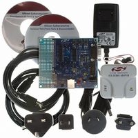
KIT DEV FOR C8051F326/7
Manufacturer
Silicon Laboratories Inc
Type
MCUr
Specifications of C8051F326DK
Contents
Evaluation Board, Power Supply, USB Cables, Adapter and Documentation
Processor To Be Evaluated
C8051F326/F327
Interface Type
USB
Silicon Manufacturer
Silicon Labs
Core Architecture
8051
Silicon Core Number
C8051F326
Silicon Family Name
C8051F32x
Lead Free Status / RoHS Status
Contains lead / RoHS non-compliant
For Use With/related Products
Silicon Laboratories C8051F326, C8051F327
Lead Free Status / Rohs Status
Lead free / RoHS Compliant
Other names
336-1306


6.1. System Clock Sources
The C8051F320 device installed on the target board features a calibrated programmable internal oscillator which is
enabled as the system clock source on reset. After reset, the internal oscillator operates at a frequency of 1.5 MHz
(±1.5%) by default but may be configured by software to operate at other frequencies. Therefore, in many
applications an external oscillator is not required. However, if you wish to operate the C8051F320 device at a
frequency not available with the internal oscillator, an external crystal may be used. Refer to the C8051F32x
datasheet for more information on configuring the system clock source.
The target board is designed to facilitate the installation of an external crystal. Remove shorting blocks at headers
J9 and J10 and install the crystal at the pads marked Y1. Install a 10 MΩ resistor at R9 and install capacitors at
C14 and C15 using values appropriate for the crystal you select. Refer to the C8051F32x datasheet for more
information on the use of external oscillators.
6.2. Switches and LEDs
Three switches are provided on the target board. Switch SW1 is connected to the RESET pin of the C8051F320.
Pressing SW1 puts the device into its hardware-reset state. Switch SW2 and SW3 are connected to the
C8051F320’s general purpose I/O (GPIO) pins through headers. Pressing SW2 or SW3 generates a logic low
signal on the port pin. Remove the shorting blocks from the header to disconnect SW2 and SW3 from the port pins.
The port pin signals are also routed to pins on the J1 I/O connector. See Table 1 for the port pins and headers
corresponding to each switch.
Three LEDs are also provided on the target board. The red LED labeled PWR is used to indicate a power
connection to the target board. The green LEDs labeled with port pin names areconnected to the C8051F320’s
GPIO pins through headers. Remove the shorting blocks from the header to disconnect the LEDs from the port pin.
The port pin signals are also routed to pins on the J1 I/O connector. See Table 1 for the port pins and headers
corresponding to each LED.
Also included on the C8051F320 target board is a 10 KΩ Thumb-wheel Rotary Potentiometer, part number R14.
The Potentiometer is connected to the C8051F320’s GPIO pin through a header. Remove the shorting block from
the header to disconnect the Potentiometer from the port pin. The port pin signal is also routed to a pin on the J1 I/
O connector. See Table 1 for the port pin and header corresponding to the Potentiometer.
Potentiometer
Description
Green LED
Green LED
Table 1. Target Board I/O Descriptions
Red LED
SW1
SW2
SW3
Rev. 0.8
Reset
PWR
P2.0
P2.1
P2.2
P2.3
R14
I/O
Header
J3[1–2]
J3[3–4]
J3[5–6]
J3[7–8]
none
none
J13
C8051F32x-DK
7
Related parts for C8051F326DK
Image
Part Number
Description
Manufacturer
Datasheet
Request
R

Part Number:
Description:
SMD/C°/SINGLE-ENDED OUTPUT SILICON OSCILLATOR
Manufacturer:
Silicon Laboratories Inc
Part Number:
Description:
Manufacturer:
Silicon Laboratories Inc
Datasheet:
Part Number:
Description:
N/A N/A/SI4010 AES KEYFOB DEMO WITH LCD RX
Manufacturer:
Silicon Laboratories Inc
Datasheet:
Part Number:
Description:
N/A N/A/SI4010 SIMPLIFIED KEY FOB DEMO WITH LED RX
Manufacturer:
Silicon Laboratories Inc
Datasheet:
Part Number:
Description:
N/A/-40 TO 85 OC/EZLINK MODULE; F930/4432 HIGH BAND (REV E/B1)
Manufacturer:
Silicon Laboratories Inc
Part Number:
Description:
EZLink Module; F930/4432 Low Band (rev e/B1)
Manufacturer:
Silicon Laboratories Inc
Part Number:
Description:
I°/4460 10 DBM RADIO TEST CARD 434 MHZ
Manufacturer:
Silicon Laboratories Inc
Part Number:
Description:
I°/4461 14 DBM RADIO TEST CARD 868 MHZ
Manufacturer:
Silicon Laboratories Inc
Part Number:
Description:
I°/4463 20 DBM RFSWITCH RADIO TEST CARD 460 MHZ
Manufacturer:
Silicon Laboratories Inc
Part Number:
Description:
I°/4463 20 DBM RADIO TEST CARD 868 MHZ
Manufacturer:
Silicon Laboratories Inc
Part Number:
Description:
I°/4463 27 DBM RADIO TEST CARD 868 MHZ
Manufacturer:
Silicon Laboratories Inc
Part Number:
Description:
I°/4463 SKYWORKS 30 DBM RADIO TEST CARD 915 MHZ
Manufacturer:
Silicon Laboratories Inc
Part Number:
Description:
N/A N/A/-40 TO 85 OC/4463 RFMD 30 DBM RADIO TEST CARD 915 MHZ
Manufacturer:
Silicon Laboratories Inc
Part Number:
Description:
I°/4463 20 DBM RADIO TEST CARD 169 MHZ
Manufacturer:
Silicon Laboratories Inc