C8051F326DK Silicon Laboratories Inc, C8051F326DK Datasheet
C8051F326DK
Specifications of C8051F326DK


Related parts for C8051F326DK

C8051F326DK Summary of contents
Page 1
USB Function Controller - USB specification 2.0 compliant - Full speed (12 Mbps) or low speed (1.5 Mbps) operation - Integrated clock recovery; no external crystal required for full speed or low speed - Supports three fixed-function endpoints - 256 ...
Page 2
C8051F326/7 2 Rev. 1.1 ...
Page 3
Table of Contents 1. System Overview.................................................................................................... 13 1.1. CIP-51™ Microcontroller Core.......................................................................... 17 1.1.1. Fully 8051 Compatible.............................................................................. 17 1.1.2. Improved Throughput ............................................................................... 17 1.1.3. Additional Features .................................................................................. 18 1.2. On-Chip Memory............................................................................................... 19 1.3. Universal Serial Bus Controller ......................................................................... 20 1.4. Voltage ...
Page 4
C8051F326/7 7.5. Flash Error Reset.............................................................................................. 60 7.6. Software Reset ................................................................................................. 60 7.7. USB Reset ........................................................................................................ 60 8. Flash Memory ....................................................................................................... 63 8.1. Programming The Flash Memory ..................................................................... 63 8.1.1. Flash Lock and Key Functions ................................................................. 63 8.1.2. Flash Erase Procedure............................................................................. ...
Page 5
Endpoint1 IN............................................................................... 108 12.12.1.Endpoint1 IN Interrupt or Bulk Mode.................................................... 108 12.12.2.Endpoint1 IN Isochronous Mode.......................................................... 108 12.13.Controlling Endpoint1 OUT........................................................................... 112 12.13.1.Endpoint1 OUT Interrupt or Bulk Mode................................................ 112 12.13.2.Endpoint1 OUT Isochronous Mode...................................................... 112 13. UART0.................................................................................................................... 117 13.1.Baud Rate Generator ..................................................................................... 118 ...
Page 6
C8051F326/7 6 Rev. 1.1 ...
Page 7
List of Figures 1. System Overview Figure 1.1. C8051F326 Block Diagram .................................................................... 14 Figure 1.2. C8051F327 Block Diagram .................................................................... 15 Figure 1.3. Typical Connections for the C8051F326................................................ 16 Figure 1.4. Typical Connections for the C8051F327................................................ 16 Figure 1.5. Comparison of ...
Page 8
C8051F326/7 Figure 13.2. UART0 Timing Without Parity or Extra Bit.......................................... 120 Figure 13.3. UART0 Timing With Parity ................................................................. 120 Figure 13.4. UART0 Timing With Extra Bit ............................................................. 120 Figure 13.5. Typical UART Interconnect Diagram.................................................. 121 Figure 13.6. UART Multi-Processor Mode ...
Page 9
List of Tables 1. System Overview Table 1.1. Product Selection Guide ......................................................................... 13 2. Absolute Maximum Ratings Table 2.1. Absolute Maximum Ratings .................................................................... 23 3. Global DC Electrical Characteristics Table 3.1. Global DC Electrical Characteristics ....................................................... 24 4. Pinout and ...
Page 10
C8051F326/7 10 Rev. 1.1 ...
Page 11
List of Registers SFR Definition 5.1. REG0CN: Voltage Regulator Control . . . . . . . . . . . . . . . . . . . . . . 34 SFR Definition 6.1. DPL: Data Pointer Low ...
Page 12
C8051F326/7 USB Register Definition 12.12. OUT1INT: USB0 Out Endpoint Interrupt . . . . . . . . . . 101 USB Register Definition 12.13. CMINT: USB0 Common Interrupt . . . . . . . . . . . ...
Page 13
System Overview C8051F326/7 devices are fully integrated mixed-signal system-on-a-chip MCUs. Highlighted features are listed below. Refer to Table 1.1 for specific product feature selection. • High-speed pipelined 8051-compatible microcontroller core ( MIPS) • In-system, full-speed, non-intrusive debug ...
Page 14
C8051F326/7 5.0 V Voltage Enable REGIN IN Regulator OUT Analog/Digital VDD Power GND C2D Debug HW /RST/C2CK Brown- POR Out Low Freq Oscillator XTAL2 12 MHz Internal x4 2 Oscillator 1,2,3,4 2 USB Clock Clock XTAL2 Recovery D+ USB Transceiver ...
Page 15
V Voltage Enable REGIN IN Regulator OUT Analog/Digital VDD Power GND C2D Debug HW /RST/C2CK Brown- POR Out Low Freq Oscillator XTAL2 12 MHz Internal x4 2 Oscillator 1,2,3,4 2 USB Clock Clock Recovery XTAL2 D+ USB Transceiver Controller ...
Page 16
C8051F326/7 Figure 1.3. Typical Connections for the C8051F326 Figure 1.4. Typical Connections for the C8051F327 16 Rev. 1.1 ...
Page 17
CIP-51™ Microcontroller Core 1.1.1. Fully 8051 Compatible The C8051F326/7 family utilizes Silicon Laboratories' proprietary CIP-51 microcontroller core. The CIP-51 is fully compatible with the MCS-51™ instruction set; standard 803x/805x assemblers and compilers can be used to develop software. The ...
Page 18
C8051F326/7 1.1.3. Additional Features The C8051F326/7 SoC family includes several key enhancements to the CIP-51 core and peripherals to improve performance and ease of use in end applications. The extended interrupt handler provides 8 interrupt sources into the CIP-51. An ...
Page 19
On-Chip Memory The CIP-51 has a standard 8051 program and data address configuration. It includes 256 bytes of data RAM, with the upper 128 bytes dual-mapped. Indirect addressing accesses the upper 128 bytes of general purpose RAM, and direct ...
Page 20
C8051F326/7 1.3. Universal Serial Bus Controller The Universal Serial Bus Controller (USB0 USB 2.0 peripheral with integrated transceiver and end- point FIFO RAM. The controller supports both full and low speed modes. A total of three endpoint pipes ...
Page 21
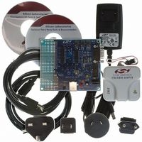
... All the peripherals (except for the USB) are stalled when the MCU is halted, during single stepping breakpoint in order to keep them synchronized. The C8051F326DK development kit provides all the hardware and software necessary to develop applica- tion code and perform in-circuit debugging with the C8051F326/7 MCUs. The kit includes a Windows development environment, a serial adapter for connecting to the C2 port, and a target application board ...
Page 22
C8051F326/7 1.6. Programmable Digital I/O C8051F326/7 devices include 15 I/O pins (one byte-wide Port, one 6-bit-wide and one 1-bit-wide Port). The C8051F326/7 Ports behave like typical 8051 Ports with a few enhancements. Each Port pin may be configured as a ...
Page 23
Absolute Maximum Ratings Table 2.1. Absolute Maximum Ratings Parameter Ambient Temperature under Bias Storage Temperature Voltage on any Port I/O Pin or RST with Respect to GND Voltage on VDD or VIO with Respect to GND Maximum Total Current ...
Page 24
C8051F326/7 3. Global DC Electrical Characteristics Table 3.1. Global DC Electrical Characteristics –40 to +85 °C, 25 MHz System Clock unless otherwise specified. Parameter 1,2 I/O Supply Voltage (VIO) 3 Core Supply Voltage (VDD) Core Supply Current with CPU VDD ...
Page 25
Pinout and Package Definitions Table 4.1. Pin Definitions for the C8051F326/7 Pin Numbers Name ‘F326 ‘F327 VDD 6 6 VIO 5 — GND 2 3 RST C2CK P3. C2D REGIN 7 7 VBUS 8 8 ...
Page 26
C8051F326/7 Table 4.1. Pin Definitions for the C8051F326/7 (Continued) Pin Numbers Name ‘F326 ‘F327 N.C. pins ...
Page 27
P0.0 1 GND C8051F326 D- 4 VIO 5 VDD 6 REGIN 7 Figure 4.1. C8051F326 QFN-28 Pinout Diagram (Top View) C8051F326/7 Top View GND Rev. 1.1 21 N.C. 20 N.C. 19 P2.0 18 P2.1 17 P2.4 16 ...
Page 28
C8051F326/7 P0.1 1 P0.0 2 GND VDD 6 REGIN 7 Figure 4.2. C8051F327 QFN-28 Pinout Diagram (Top View) 28 C8051F327 Top View GND Rev. 1.1 21 N.C. 20 N.C. 19 P2.0 18 P2.1 17 P2.4 ...
Page 29
Figure 4.3. QFN-28 Package Drawing Table 4.2. QFN-28 Package Dimensions Dimension Min Typ A 0.80 0.90 A1 0.00 0.02 A3 0.25 REF b 0.18 0.23 D 5.00 BSC. D2 2.90 3.15 e 0.50 BSC. E 5.00 BSC. E2 2.90 3.15 ...
Page 30
C8051F326/7 Figure 4.4. QFN-28 Recommended PCB Land Pattern Table 4.3. QFN-28 PCB Land Pattern Dimensions Dimension Min C1 4.80 C2 4.80 E 0.50 X1 0.20 Notes: General 1. All dimensions shown are in millimeters (mm) unless otherwise noted. 2. Dimensioning ...
Page 31
Voltage Regulator (REG0) C8051F326/7 devices include a voltage regulator (REG0). When enabled, the REG0 output appears on the VDD pin and can be used to power external devices. REG0 can be enabled/disabled by software using bit REGEN in register ...
Page 32
C8051F326/7 VBUS From VBUS REGIN 1.0 µF 0.1 µ VDD Power Net 0.1 µF 1.0 µF Figure 5.1. REG0 Configuration: USB Bus-Powered VBUS From VBUS From 5 V REGIN Power Net 0.1 µF 1.0 µ ...
Page 33
C8051F326/7 VBUS From VBUS REGIN 0.1 µF 1.0 µF From 3 V VDD Power Net Figure 5.3. REG0 Configuration: USB Self-Powered, Regulator Disabled C8051F326/7 VBUS From 5 V REGIN Power Net 0.1 µF 1.0 µ VDD Power ...
Page 34
C8051F326/7 SFR Definition 5.1. REG0CN: Voltage Regulator Control R/W R R/W REGDIS VBSTAT VBPOL Bit7 Bit6 Bit5 Bit7: REGDIS: Voltage Regulator Disable. 0: Voltage Regulator Enabled. 1: Voltage Regulator Disabled. Bit6: VBSTAT: VBUS Signal Status. 0: VBUS signal currently absent ...
Page 35
CIP-51 Microcontroller The MCU system controller core is the CIP-51 microcontroller. The CIP-51 is fully compatible with the MCS-51™ instruction set; standard 803x/805x assemblers and compilers can be used to develop soft- ware. The MCU family has a superset ...
Page 36
C8051F326/7 Performance The CIP-51 employs a pipelined architecture that greatly increases its instruction throughput over the stan- dard 8051 architecture standard 8051, all instructions except for MUL and DIV take system clock cycles to execute, ...
Page 37
MOVX Instruction and Program Memory The MOVX instruction is typically used to access external data memory (Note: the C8051F326/7 does not support off-chip data or program memory). In the CIP-51, the MOVX write instruction is used to accesses external ...
Page 38
C8051F326/7 Table 6.1. CIP-51 Instruction Set Summary (Continued) Mnemonic Description ORL direct, #data OR immediate to direct byte XRL A, Rn Exclusive-OR Register to A XRL A, direct Exclusive-OR direct byte to A XRL A, @Ri Exclusive-OR indirect RAM to ...
Page 39
Table 6.1. CIP-51 Instruction Set Summary (Continued) Mnemonic Description CLR bit Clear direct bit SETB C Set Carry SETB bit Set direct bit CPL C Complement Carry CPL bit Complement direct bit ANL C, bit AND direct bit to Carry ...
Page 40
C8051F326/7 Notes on Registers, Operands and Addressing Modes Register R0-R7 of the currently selected register bank. @Ri - Data RAM location addressed indirectly through R0 or R1. rel - 8-bit, signed (2s complement) offset relative to the first ...
Page 41
Memory Organization The memory organization of the CIP-51 System Controller is similar to that of a standard 8051. There are two separate memory spaces: program memory and data memory. Program and data memory share the same address space but ...
Page 42
C8051F326/7 6.2.2. Data Memory The CIP-51 includes 256 of internal RAM mapped into the data memory space from 0x00 through 0xFF. The lower 128 bytes of data memory are used for general purpose registers and scratch pad memory. Either direct ...
Page 43
Special Function Registers The direct-access data memory locations from 0x80 to 0xFF constitute the special function registers (SFRs). The SFRs provide control and data exchange with the CIP-51's resources and peripherals. The CIP-51 duplicates the SFRs found in a ...
Page 44
C8051F326/7 Table 6.3. Special Function Registers (Continued) SFRs are listed in alphabetical order. All undefined SFR locations are reserved. Register Address Description EIE2 0xE7 Extended Interrupt Enable 2 EIP1 0xF6 Extended Interrupt Priority 1 EIP2 0xF7 Extended Interrupt Priority 2 ...
Page 45
Register Descriptions Following are descriptions of SFRs related to the operation of the CIP-51 System Controller. Reserved bits should not be set to logic l. Future product versions may use these bits to implement new features in which case ...
Page 46
C8051F326/7 SFR Definition 6.4. PSW: Program Status Word R/W R/W R Bit7 Bit6 Bit5 Bit7: CY: Carry Flag. This bit is set when the last arithmetic operation resulted in a carry (addition borrow (subtraction). It ...
Page 47
SFR Definition 6. Register R/W R/W R/W B.7 B.6 B.5 Bit7 Bit6 Bit5 Bits7– Register. This register serves as a second accumulator for certain arithmetic operations. R/W R/W R/W R/W B.4 B.3 B.2 B.1 Bit4 Bit3 ...
Page 48
C8051F326/7 6.3. Interrupt Handler The CIP-51 includes an extended interrupt system supporting a total of 8 interrupt sources with two priority levels. The allocation of interrupt sources between on-chip peripherals and external inputs pins varies according to the specific version ...
Page 49
External Interrupts The /INT0 external interrupt source can be configured as edge or level sensitive. The IT0 bit (TCON.0, see Figure 14.1 on Page 128) selects level or edge sensitivity. When global port I/O inputs are enabled, /INT0 will ...
Page 50
C8051F326/7 Table 6.5. Interrupt Summary Interrupt Interrupt Source Vector Reset 0x0000 External Interrupt 0 0x0003 (/INT0) Timer 0 Overflow 0x000B External Interrupt 1 0x0013 (/INT1) Timer 1 Overflow 0x001B UART0 0x0023 USB0 0x0043 VBUS Level 0x007B *Note: See Section “12.8. ...
Page 51
SFR Definition 6.7. IE: Interrupt Enable R — — Bit7 Bit6 Bit5 Bit7: EA: Enable All Interrupts. This bit globally enables/disables all interrupts. It overrides the individual interrupt mask set- tings. 0: Disable all interrupt sources. 1: ...
Page 52
C8051F326/7 SFR Definition 6.8. IP: Interrupt Priority — — — Bit7 Bit6 Bit5 Bit7–5: Unused. Read = 100b. Write = don't care. Bit4: PS0: UART0 Interrupt Priority Control. This bit sets the priority of the UART0 interrupt. ...
Page 53
SFR Definition 6.9. EIE1: Extended Interrupt Enable — — — Bit7 Bit6 Bit5 Bit7–2: Unused. Read = 000000b. Write = don’t care. Bit1: EUSB0: Enable USB0 Interrupt. This bit sets the masking of the USB0 interrupt. ...
Page 54
C8051F326/7 SFR Definition 6.12. EIP2: Extended Interrupt Priority — — — Bit7 Bit6 Bit5 Bits7–1: Unused. Read = 0000000b. Write = don’t care. Bit0: PVBUS: VBUS Level Interrupt Priority Control. This bit sets the priority of ...
Page 55
Power Management Modes The CIP-51 core has two software programmable power management modes: Idle and Stop. Idle mode halts the CPU while leaving the peripherals and clocks active. In Stop mode, the CPU is halted, all inter- rupts, are ...
Page 56
C8051F326/7 SFR Definition 6.13. PCON: Power Control R/W R/W R/W GF5 GF4 GF3 Bit7 Bit6 Bit5 Bits7–2: GF5-GF0: General Purpose Flags 5-0. These are general purpose flags for use under software control. Bit1: STOP: Stop Mode Select. Setting this bit ...
Page 57
Reset Sources Reset circuitry allows the controller to be easily placed in a predefined default condition. On entry to this reset state, the following occur: • CIP-51 halts program execution • Special Function Registers (SFRs) are initialized to their ...
Page 58
C8051F326/7 7.1. Power-On Reset During power-up, the device is held in a reset state and the RST pin is driven low until VDD settles above Power-On Reset delay (T RST PORDelay typically less than 0.3 ms. Figure ...
Page 59
Power-Fail Reset / VDD Monitor When a power-down transition or power irregularity causes VDD to drop below V monitor will drive the RST pin low and hold the CIP- reset state (see Figure 7.2). When VDD returns ...
Page 60
C8051F326/7 7.3. External Reset The external RST pin provides a means for external circuitry to force the device into a reset state. Assert- ing an active-low signal on the RST pin generates a reset; an external pullup and/or decoupling of ...
Page 61
SFR Definition 7.2. RSTSRC: Reset Source R USBRSF FERROR — SWRSF Bit7 Bit6 Bit5 Bit7: USBRSF: USB Reset Flag 0: Read: Last reset was not a USB reset; Write: USB resets disabled. 1: Read: Last reset was a ...
Page 62
C8051F326/7 Table 7.1. Reset Electrical Characteristics –40 to +85 °C unless otherwise specified. Parameter ‘F326 RST Output Voltage ‘F327 RST Output Voltage I OL RST Input High Voltage* RST Input Low Voltage* ‘F326 RST Pullup Current ...
Page 63
Flash Memory On-chip, re-programmable Flash memory is included for program code and non-volatile data storage. The Flash memory can be programmed in-system, a single byte at a time, through the C2 interface or by soft- ware using the MOVX ...
Page 64
C8051F326/7 8.1.3. Flash Write Procedure Flash bytes are programmed by software with the following sequence: Step 1. Disable interrupts (recommended). Step 2. Erase the 512-byte Flash page containing the target location, as described in Section “8.1.2. Flash Erase Procedure” on ...
Page 65
Non-volatile Data Storage The Flash memory can be used for non-volatile data storage as well as program code. This allows data such as calibration coefficients to be calculated and stored at run time. Data is written using the MOVX ...
Page 66
C8051F326/7 Locked when any other FLASH pages are locked Access limit set according to the FLASH security lock byte Figure 8.1. Flash Program Memory Map and Security Byte SFR Definition 8.1. PSCTL: Program Store R/W Control R/W R/W R/W — ...
Page 67
SFR Definition 8.2. FLKEY: Flash Lock and Key R/W R/W R/W Bit7 Bit6 Bit5 Bits7–0: FLKEY: Flash Lock and Key Register Write: This register must be written to before Flash writes or erases can be performed. Flash remains locked until ...
Page 68
C8051F326/7 68 Rev. 1.1 ...
Page 69
External RAM The C8051F326/7 devices include 1280 bytes of on-chip XRAM. This XRAM space is split into user RAM (addresses 0x0000–0x03FF) and USB0 FIFO space. The USB0 FIFO space is only accessible through the USB FIFO registers ...
Page 70
C8051F326/7 9.2. Accessing USB FIFO Space The upper 256 bytes of XRAM functions as USB FIFO space. Figure 9.2 shows an expanded view of the FIFO space and user XRAM. FIFO space is accessed via USB FIFO registers; see Section ...
Page 71
Oscillators C8051F326/7 devices include a programmable internal oscillator, an external clock input circuit, a low fre- quency internal oscillator, and a 4x Clock Multiplier. The internal oscillator can be enabled/disabled and calibrated using the OSCICN and OSCICL registers, as ...
Page 72
C8051F326/7 10.1.1. Adjusting the Internal Oscillator on C8051F326/7 Devices The OSCICL reset value is factory calibrated to result MHz internal oscillator with a ±1.5% accu- racy; this frequency is suitable for use as the USB clock (see ...
Page 73
SFR Definition 10.2. OSCICL: Internal Oscillator Calibration R/W R/W R/W — — — Bit7 Bit6 Bit5 Bits4–0: OSCCAL: Oscillator Calibration Value These bits determine the internal oscillator period. Note: If the sum of the reset value of OSCCAL and ΔOSCCAL ...
Page 74
C8051F326/7 10.2. Internal Low-Frequency (L-F) Oscillator C8051F326/7 devices include a low-frequency oscillator. The OSCLCN register (see SFR Definition 10.3) is used to enabled the oscillator. SFR Definition 10.3. OSCLCN: Internal L-F Oscillator Control R OSCLEN — — Bit7 ...
Page 75
Clock Multiplier The 4x Clock Multiplier allows a 12 MHz oscillator to generate the 48 MHz clock required for Full Speed USB communication (see Section “12.4. USB Clock Configuration” on page 94). A divided version of the Multiplier ...
Page 76
C8051F326/7 10.5. System and USB Clock Selection The internal oscillator requires little start-up time and may be selected as the system or USB clock immedi- ately following the OSCICN write that enables the internal oscillator. If the external clock is ...
Page 77
SFR Definition 10.5. CLKSEL: Clock Select R/W R/W R/W — — USBCLK Bit7 Bit6 Bit5 Bits7–6: Unused. Read = 0b. Write = don’t care. Bits5–4: USBCLK1–0: USB Clock Select These bits select the clock supplied to USB0. When operating USB0 ...
Page 78
C8051F326/7 Table 10.3. Internal Oscillator Electrical Characteristics –40 to +85 °C unless otherwise specified. Parameter Internal High-Frequency Oscillator Internal Oscillator Frequency Reset Frequency Internal Oscillator Supply OSCICN Current (from VDD) 1 USB Clock Frequency Full Speed Mode Low ...
Page 79
Port Input/Output On-Chip digital resources are available through 15 I/O pins. Port pins are organized as shown in Figure 11.1. Each of the Port pins can be used as general-purpose I/O (GPIO). Some port pins can be dedicated to ...
Page 80
C8051F326/7 /WEAK-PULLUP PUSH-PULL Logic 0 PORT-OUTPUT INPUTEN PORT-INPUT Figure 11.2. Port I/O Cell Block Diagram 80 Supply Supply (WEAK) GND Rev. 1.1 PORT PAD ...
Page 81
Port I/O Initialization Port I/O initialization consists of the following steps: Step 1. Select if the port pin will be used as an output or input. Step 2. If output, select the output mode: open-drain or push-pull. Step 3. ...
Page 82
C8051F326/7 SFR Definition 11.1. GPIOCN: Global Port I/O Control R/W R/W R WEAKPUD INPUTEN — Bit7 Bit6 Bit5 Bit7: WEAKPUD: Port I/O Weak Pullup Disable. 0: Weak Pullups enabled (except for I/O pins with Port latches set to logic 0 ...
Page 83
SFR Definition 11.4. P2: Port2 R/W R/W R/W — — P2.5 Bit7 Bit6 Bit5 Bits7–6: Unused. Read = 00b. Write = don’t care. Bits5–0: P2.[5:0] Write - Output appears on I/O pins. 0: Logic Low Output. 1: Logic High Output ...
Page 84
C8051F326/7 SFR Definition 11.7. P3MDOUT: Port3 Output Mode R/W R/W R/W — — — Bit7 Bit6 Bit5 Bits7–1: Unused. Read = 0000000b. Write = don’t care. Bit0: Output Configuration Bit for P3.0: 0: P3.0 Output is open-drain. 1: P3.0 Output ...
Page 85
Table 11.1. Port I/O DC Electrical Characteristics (C8051F326) VDD = 2.7 to 3.6 V, –40 to +85 °C unless otherwise specified Parameter Output High Voltage IOH = –10 µA; Port I/O push-pull IOH = –3 mA; Port I/O push-pull IOH ...
Page 86
C8051F326 OTES 86 Rev. 1.1 ...
Page 87
Universal Serial Bus Controller (USB0) C8051F326/7 devices include a complete Full/Low Speed USB function for USB peripheral implementa- tions*. The USB Function Controller (USB0) consists of a Serial Interface Engine (SIE), USB Transceiver (including matching resistors and configurable pullup ...
Page 88
C8051F326/7 12.1. Endpoint Addressing A total of three endpoint pipes are available. The control endpoint (Endpoint0) always functions as a bi-directional IN/OUT endpoint. Endpoint 1 is implemented byte IN pipe and a 128 byte OUT pipe: Table ...
Page 89
USB Register Definition 12.1. USB0XCN: USB0 Transceiver Control R/W R/W R/W PREN PHYEN SPEED PHYTST1 PHYTST0 DFREC Bit7 Bit6 Bit5 Bit7: PREN: Internal Pullup Resistor Enable The location of the pullup resistor (D+ or D-) is determined by the SPEED ...
Page 90
C8051F326/7 12.3. USB Register Access The USB0 controller registers listed in Table 12.2 are accessed through two SFRs: USB0 Address (USB0ADR) and USB0 Data (USB0DAT). The USB0ADR register selects which USB register is targeted by reads/writes of the USB0DAT register. ...
Page 91
USB Register Definition 12.2. USB0ADR: USB0 Indirect Address R/W R/W R/W BUSY AUTORD Bit7 Bit6 Bit5 Bits7: BUSY: USB0 Register Read Busy Flag This bit is used during indirect USB0 register accesses. Software should write ‘1’ to this bit to ...
Page 92
C8051F326/7 USB Register Definition 12.3. USB0DAT: USB0 Data R/W R/W R/W Bit7 Bit6 Bit5 This SFR is used to indirectly read and write USB0 registers. Write Procedure: 1. Poll for BUSY (USB0ADR.7) => ‘0’. 2. Load the target USB0 register ...
Page 93
Table 12.2. USB0 Controller Registers USB Register USB Register Name Address IN1INT 0x02 OUT1INT 0x04 CMINT 0x06 IN1IE 0x07 OUT1IE 0x09 CMIE 0x0B FADDR 0x00 POWER 0x01 FRAMEL 0x0C FRAMEH 0x0D INDEX 0x0E CLKREC 0x0F FIFOn 0x20-0x21 E0CSR 0x11 EINCSRL ...
Page 94
C8051F326/7 12.4. USB Clock Configuration USB0 is capable of communication as a Full or Low Speed USB function. Communication speed is selected via the SPEED bit in SFR USB0XCN. When operating as a Low Speed function, the USB0 clock must ...
Page 95
FIFO Management 256 bytes of on-chip XRAM are used as FIFO space for USB0. This FIFO space is split between Endpoint0 and Endpoint1 as shown in Figure 12.3. FIFO space allocated for Endpoint1 is split into an IN and ...
Page 96
C8051F326/7 12.5.1. FIFO Access Each endpoint FIFO is accessed through a corresponding FIFOn register. A read of an endpoint FIFOn register unloads one byte from the FIFO; a write of an endpoint FIFOn register loads one byte into the end- ...
Page 97
Function Addressing The FADDR register holds the current USB0 function address. Software should write the host-assigned 7-bit function address to the FADDR register when received as part of a SET_ADDRESS command. A new address written to FADDR will not ...
Page 98
C8051F326/7 12.7. Function Configuration and Control The USB register POWER (Figure 12.8) is used to configure and control USB0 at the device level (enable/ disable, Reset/Suspend/Resume handling, etc.). USB Reset: The USBRST bit (POWER.3) is set to ‘1’ by hardware ...
Page 99
USB Register Definition 12.8. POWER: USB0 Power R/W R/W R/W ISOUD - - USBINH Bit7 Bit6 Bit5 Bit7: ISOUD: ISO Update This bit affects all IN Isochronous endpoints. 0: When software writes INPRDY = ‘1’, USB0 will send the packet ...
Page 100
C8051F326/7 USB Register Definition 12.9. FRAMEL: USB0 Frame Number Low Bit7 Bit6 Bit5 Bits7–0: Frame Number Low This register contains bits7-0 of the last received frame number. USB Register Definition 12.10. FRAMEH: USB0 Frame Number High R ...
Page 101
Interrupts The read-only USB0 interrupt flags are located in the USB registers shown in Figure 12.11 through Figure 12.13. The associated interrupt enable bits are located in the USB registers shown in Figure 12.14 through Figure 12.16. A USB0 ...
Page 102
C8051F326/7 USB Register Definition 12.13. CMINT: USB0 Common Interrupt — — — Bit7 Bit6 Bit5 Bits7–4: Unused. Read = 0000b. Write = don’t care. Bit3: SOF: Start of Frame Interrupt Set by hardware when a SOF token ...
Page 103
USB Register Definition 12.15. OUT1IE: USB0 Out Endpoint Interrupt Enable R/W R/W R/W — — — Bit7 Bit6 Bit5 Bits7–2: Unused. Read = 000000b. Write = don’t care. Bit1: OUT1E: OUT Endpoint 1 Interrupt Enable 0: OUT Endpoint 1 interrupt ...
Page 104
C8051F326/7 12.9. The Serial Interface Engine The Serial Interface Engine (SIE) performs all low level USB protocol tasks, interrupting the processor when data has successfully been transmitted or received. When receiving data, the SIE will interrupt the processor when a ...
Page 105
IN Transactions When a SETUP request is received that requires USB0 to transmit data to the host, one or more IN requests will be sent by the host. For the first IN transaction, firmware should load an IN packet ...
Page 106
C8051F326/7 USB Register Definition 12.17. E0CSR: USB0 Endpoint0 Control R/W R/W R/W SSUEND SOPRDY SDSTL Bit7 Bit6 Bit5 Bit7: SSUEND: Serviced Setup End Write: Software should set this bit to ‘1’ after servicing a Setup End (bit SUEND) event. Hardware ...
Page 107
USB Register Definition 12.18. E0CNT: USB0 Endpoint 0 Data Count Bit7 Bit6 Bit5 Bit7: Unused. Read = 0. Write = don’t care. Bits6–0: E0CNT: Endpoint 0 Data Count This 7-bit number indicates the number of received ...
Page 108
C8051F326/7 12.11. Configuring Endpoint1 Endpoint1 is configured and controlled through a set of control/status registers: IN registers EINCSRL and EINCSRH, and OUT registers EOUTCSRL and EOUTCSRH. The endpoint control/status registers are mapped into the USB register address space based on ...
Page 109
Hardware will automatically reset INPRDY (EINCSRL.0) to ‘0’ when a packet slot is open in the endpoint FIFO. Note that if double buffering is enabled for the endpoint possible for firmware to load two pack- ets into the ...
Page 110
C8051F326/7 USB Register Definition 12.19. EINCSRL: USB0 IN Endpoint Control Low Byte R W R/W — CLRDT STSTL Bit7 Bit6 Bit5 Bit7: Unused. Read = 0. Write = don’t care. Bit6: CLRDT: Clear Data Toggle. Write: Software should write ‘1’ ...
Page 111
USB Register Definition 12.20. EINCSRH: USB0 IN Endpoint Control High Byte R/W R/W R DBIEN ISO — Bit7 Bit6 Bit5 Bit7: DBIEN: IN Endpoint Double-buffer Enable. 0: Double-buffering disabled for the selected IN endpoint. 1: Double-buffering enabled for the selected ...
Page 112
C8051F326/7 12.13. Controlling Endpoint1 OUT Endpoint1 OUT is managed via USB registers EOUTCSRL and EOUTCSRH. It can be used for Interrupt, Bulk, or Isochronous transfers. Isochronous (ISO) mode is enabled by writing ‘1’ to the ISO bit in register EOUTCSRH. ...
Page 113
USB Register Definition 12.21. EOUTCSRL: USB0 OUT Endpoint Control Low Byte W R/W R/W CLRDT STSTL SDSTL Bit7 Bit6 Bit5 Bit7: CLRDT: Clear Data Toggle Write: Software should write ‘1’ to this bit to reset the OUT endpoint data toggle ...
Page 114
C8051F326/7 USB Register Definition 12.22. EOUTCSRH: USB0 OUT Endpoint Control High Byte R/W R/W R/W DBOEN ISO — Bit7 Bit6 Bit5 Bit7: DBOEN: Double-buffer Enable 0: Double-buffering disabled for the selected OUT endpoint. 1: Double-buffering enabled for the selected OUT ...
Page 115
Table 12.4. USB Transceiver Electrical Characteristics V = 3.0 to 3.6 V, –40 to +85 °C unless otherwise specified. DD Parameters Symbol USB Operating Current Transmitter Output High Voltage V OH Output Low Voltage V OL Output Crossover Point V ...
Page 116
C8051F326/7 116 Rev. 1.1 ...
Page 117
UART0 UART0 is an asynchronous, full duplex serial port offering a variety of data formatting options. A dedicated baud rate generator with a 16-bit timer and selectable prescaler is included, which can generate a wide range of baud rates ...
Page 118
C8051F326/7 13.1. Baud Rate Generator The UART0 baud rate is generated by a dedicated 16-bit timer which runs from either the controller’s core clock (SYSCLK) or the USB Clock (USBCLK), and has prescaler options 12, or 48. ...
Page 119
Table 13.1. Baud Rate Generator Settings for Standard Baud Rates Target Baud Actual Baud Baud Rate Rate (bps) Rate (bps) Error 230400 230769 0.16% 115200 115385 0.16% 57600 57692 0.16% 28800 28846 0.16% 14400 14388 0.08% 9600 9600 0.0% 2400 ...
Page 120
C8051F326/7 13.2. Data Format UART0 has a number of available options for data formatting. Data transfers begin with a start bit (logic low), followed by the data bits (sent LSB-first), a parity or extra bit (if selected), and end with ...
Page 121
Configuration and Operation UART0 provides standard asynchronous, full duplex communication. It can operate in a point-to-point serial communications application node on a multi-processor serial interface. To operate in a point-to-point application, where there are only two ...
Page 122
C8051F326/7 enabled, the value of the stop bit for the oldest FIFO byte will be presented in RBX0. When the parity func- tion is enabled (PE0 = ‘1’), hardware will check the received parity bit against the selected parity type ...
Page 123
SFR Definition 13.1. SCON0: UART0 Control R/W R/W R OVR0 PERR0 — Bit7 Bit6 Bit5 Bit7: OVR0: Receive FIFO Overrun Flag. This bit is used to indicate a receive FIFO overrun condition. 0: Receive FIFO Overrun has not occurred. 1: ...
Page 124
C8051F326/7 SFR Definition 13.2. SMOD0: UART0 Mode R/W R/W R/W MCE0 S0PT1 S0PT0 Bit7 Bit6 Bit5 Bit7: MCE0: Multiprocessor Communication Enable will be activated if stop bit(s) are ‘1’ will be activated if stop bit(s) and ...
Page 125
SFR Definition 13.3. SBUF0: UART0 Data Buffer R/W R/W R/W Bit7 Bit6 Bit5 Bits7–0: SBUF0[7:0]: Serial Data Buffer Bits 7–0 (MSB–LSB) This SFR is used to both send data from the UART and to read received data from the UART0 ...
Page 126
C8051F326/7 SFR Definition 13.5. SBRLH0: UART0 Baud Rate Generator High Byte R/W R/W R/W Bit7 Bit6 Bit5 Bits7-0: SBRLH0[7:0]: High Byte of reload value for UART0 Baud Rate Generator. SFR Definition 13.6. SBRLL0: UART0 Baud Rate Generator Low Byte R/W ...
Page 127
Timers Each MCU includes two 16-bit timers compatible with those found in the standard 8051. These timers can be used to measure time intervals and generate periodic interrupt requests. Timer 0 and Timer 1 are nearly identical and have ...
Page 128
C8051F326/7 14.1.1. Mode 0: 13-bit Timer Timer 0 and Timer 1 operate as 13-bit timers in Mode 0. The following describes the configuration and operation of Timer 0. However, both timers operate identically, and Timer 1 is configured in the ...
Page 129
Mode 1: 16-bit Timer Mode 1 operation is the same as Mode 0, except that the timer registers use all 16 bits. The timers are enabled and configured in Mode 1 in the same manner as for Mode 0. ...
Page 130
C8051F326/7 14.1.4. Mode 3: Two 8-bit Timers (Timer 0 Only) In Mode 3, Timer 0 is configured as two separate 8-bit timers held in TL0 and TH0. The counter in TL0 is controlled using the Timer 0 control/status bits in ...
Page 131
SFR Definition 14.1. TCON: Timer Control R/W R/W R/W TF1 TR1 TF0 Bit7 Bit6 Bit5 Bit7: TF1: Timer 1 Overflow Flag. Set by hardware when Timer 1 overflows. This flag can be cleared by software but is auto- matically cleared ...
Page 132
C8051F326/7 SFR Definition 14.2. TMOD: Timer Mode R/W R/W R/W GATE1 Reserved T1M1 Bit7 Bit6 Bit5 Bit7: GATE1: Timer 1 Gate Control. 0: Timer 1 enabled when TR1 = 1 irrespective of /INT1 logic level. /INT1 is activated when the ...
Page 133
SFR Definition 14.3. CKCON: Clock Control R/W R/W R/W — — — Bit7 Bit6 Bit5 Bit7–4: Unused. Read = 0b. Write = don’t care. Bit3: T1M: Timer 1 Clock Select. This select the clock source supplied to Timer 1. 0: ...
Page 134
C8051F326/7 SFR Definition 14.4. TL0: Timer 0 Low Byte R/W R/W R/W Bit7 Bit6 Bit5 Bits 7–0: TL0: Timer 0 Low Byte. The TL0 register is the low byte of the 16-bit Timer 0. SFR Definition 14.5. TL1: Timer 1 ...
Page 135
C2 Interface C8051F326/7 devices include an on-chip Silicon Laboratories 2-Wire (C2) debug interface to allow Flash programming and in-system debugging with the production part installed in the end application. The C2 interface uses a clock signal (C2CK) and a ...
Page 136
C8051F326/7 C2 Register Definition 15.3. REVID: C2 Revision ID Bit7 Bit6 Bit5 This read-only register returns the 8-bit revision ID: 0x01 (Revision B). C2 Register Definition 15.4. FPCTL: C2 Flash Programming Control Bit7 Bit6 Bit5 Bits7–0 FPCTL: Flash Programming Control ...
Page 137
C2 Pin Sharing The C2 protocol allows the C2 pins to be shared with user functions so that in-system debugging and Flash programming may be performed. This is possible because C2 communication is typically performed when the device is ...
Page 138
C8051F326 OCUMENT HANGE IST Revision 0.5 to Revision 1.0 • Updated Section “1. System Overview” on page 13 and Table 1.1, “Product Selection Guide,” on page 13. - Changed “-GQ” references to “-GM” • Added Figure 1.3. ...
Page 139
N : OTES C8051F326/7 Rev. 1.1 139 ...
Page 140
... Silicon Laboratories products for any such unintended or unauthorized application, Buyer shall indemnify and hold Silicon Laboratories harmless against all claims and damages. Silicon Laboratories and Silicon Labs are trademarks of Silicon Laboratories Inc. Other products or brandnames mentioned herein are trademarks or registered trademarks of their respective holders 140 Rev ...