C8051F326DK Silicon Laboratories Inc, C8051F326DK Datasheet - Page 60
C8051F326DK
Manufacturer Part Number
C8051F326DK
Description
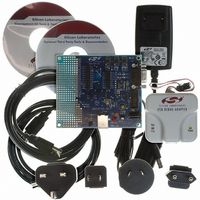
KIT DEV FOR C8051F326/7
Manufacturer
Silicon Laboratories Inc
Type
MCUr
Specifications of C8051F326DK
Contents
Evaluation Board, Power Supply, USB Cables, Adapter and Documentation
Processor To Be Evaluated
C8051F326/F327
Interface Type
USB
Silicon Manufacturer
Silicon Labs
Core Architecture
8051
Silicon Core Number
C8051F326
Silicon Family Name
C8051F32x
Lead Free Status / RoHS Status
Contains lead / RoHS non-compliant
For Use With/related Products
Silicon Laboratories C8051F326, C8051F327
Lead Free Status / Rohs Status
Lead free / RoHS Compliant
Other names
336-1306


C8051F326/7
7.3.
The external RST pin provides a means for external circuitry to force the device into a reset state. Assert-
ing an active-low signal on the RST pin generates a reset; an external pullup and/or decoupling of the RST
pin may be necessary to avoid erroneous noise-induced resets. See Table 7.1 for complete RST pin spec-
ifications. The PINRSF flag (RSTSRC.0) is set on exit from an external reset.
7.4.
The Missing Clock Detector (MCD) is a one-shot circuit that is triggered by the system clock. If more than
100 µs pass between rising edges on the system clock, the one-shot will time out and generate a reset.
After a MCD reset, the MCDRSF flag (RSTSRC.2) will read ‘1’, signifying the MCD as the reset source;
otherwise, this bit reads ‘0’. Writing a ‘1’ to the MCDRSF bit enables the Missing Clock Detector; writing a
‘0’ disables it. The state of the RST pin is unaffected by this reset.
7.5.
If a Flash read/write/erase or program read targets an illegal address, a system reset is generated. This
may occur due to any of the following:
•
•
•
•
The FERROR bit (RSTSRC.6) is set following a Flash error reset. The state of the RST pin is unaffected by
this reset.
7.6.
Software may force a reset by writing a ‘1’ to the SWRSF bit (RSTSRC.4). The SWRSF bit will read ‘1’ fol-
lowing a software forced reset. The state of the RST pin is unaffected by this reset.
7.7.
Writing ‘1’ to the USBRSF bit in register RSTSRC selects USB0 as a reset source. With USB0 selected as
a reset source, a system reset will be generated when either of the following occur:
The USBRSF bit will read ‘1’ following a USB reset. The state of the RST pin is unaffected by this reset.
60
A Flash write or erase is attempted above user code space. This occurs when PSWE is set to ‘1’ and a
MOVX write operation is attempted above address 0x3DFF.
A Flash read is attempted above user code space. This occurs when a MOVC operation is attempted
above address 0x3DFF.
A Program read is attempted above user code space. This occurs when user code attempts to branch
to an address above 0x3DFF.
A Flash read, write or erase attempt is restricted due to a Flash security setting (see Section
“8.3. Security Options” on page 65).
External Reset
Missing Clock Detector Reset
Flash Error Reset
Software Reset
USB Reset
1. RESET signaling is detected on the USB network. The USB Function Controller (USB0) must
2. The voltage on the VBUS pin matches the polarity selected by the VBPOL bit in register
be enabled for RESET signaling to be detected. See Section “12. Universal Serial Bus Con-
troller (USB0)” on page 87 for information on the USB Function Controller.
REG0CN. See Section “5. Voltage Regulator (REG0)” on page 31 for details on the VBUS
detection circuit.
Rev. 1.1
Related parts for C8051F326DK
Image
Part Number
Description
Manufacturer
Datasheet
Request
R

Part Number:
Description:
SMD/C°/SINGLE-ENDED OUTPUT SILICON OSCILLATOR
Manufacturer:
Silicon Laboratories Inc
Part Number:
Description:
Manufacturer:
Silicon Laboratories Inc
Datasheet:
Part Number:
Description:
N/A N/A/SI4010 AES KEYFOB DEMO WITH LCD RX
Manufacturer:
Silicon Laboratories Inc
Datasheet:
Part Number:
Description:
N/A N/A/SI4010 SIMPLIFIED KEY FOB DEMO WITH LED RX
Manufacturer:
Silicon Laboratories Inc
Datasheet:
Part Number:
Description:
N/A/-40 TO 85 OC/EZLINK MODULE; F930/4432 HIGH BAND (REV E/B1)
Manufacturer:
Silicon Laboratories Inc
Part Number:
Description:
EZLink Module; F930/4432 Low Band (rev e/B1)
Manufacturer:
Silicon Laboratories Inc
Part Number:
Description:
I°/4460 10 DBM RADIO TEST CARD 434 MHZ
Manufacturer:
Silicon Laboratories Inc
Part Number:
Description:
I°/4461 14 DBM RADIO TEST CARD 868 MHZ
Manufacturer:
Silicon Laboratories Inc
Part Number:
Description:
I°/4463 20 DBM RFSWITCH RADIO TEST CARD 460 MHZ
Manufacturer:
Silicon Laboratories Inc
Part Number:
Description:
I°/4463 20 DBM RADIO TEST CARD 868 MHZ
Manufacturer:
Silicon Laboratories Inc
Part Number:
Description:
I°/4463 27 DBM RADIO TEST CARD 868 MHZ
Manufacturer:
Silicon Laboratories Inc
Part Number:
Description:
I°/4463 SKYWORKS 30 DBM RADIO TEST CARD 915 MHZ
Manufacturer:
Silicon Laboratories Inc
Part Number:
Description:
N/A N/A/-40 TO 85 OC/4463 RFMD 30 DBM RADIO TEST CARD 915 MHZ
Manufacturer:
Silicon Laboratories Inc
Part Number:
Description:
I°/4463 20 DBM RADIO TEST CARD 169 MHZ
Manufacturer:
Silicon Laboratories Inc