C8051F326DK Silicon Laboratories Inc, C8051F326DK Datasheet - Page 43
C8051F326DK
Manufacturer Part Number
C8051F326DK
Description
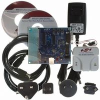
KIT DEV FOR C8051F326/7
Manufacturer
Silicon Laboratories Inc
Type
MCUr
Specifications of C8051F326DK
Contents
Evaluation Board, Power Supply, USB Cables, Adapter and Documentation
Processor To Be Evaluated
C8051F326/F327
Interface Type
USB
Silicon Manufacturer
Silicon Labs
Core Architecture
8051
Silicon Core Number
C8051F326
Silicon Family Name
C8051F32x
Lead Free Status / RoHS Status
Contains lead / RoHS non-compliant
For Use With/related Products
Silicon Laboratories C8051F326, C8051F327
Lead Free Status / Rohs Status
Lead free / RoHS Compliant
Other names
336-1306


6.2.6. Special Function Registers
The direct-access data memory locations from 0x80 to 0xFF constitute the special function registers
(SFRs). The SFRs provide control and data exchange with the CIP-51's resources and peripherals. The
CIP-51 duplicates the SFRs found in a typical 8051 implementation as well as implementing additional
SFRs used to configure and access the sub-systems unique to the MCU. This allows the addition of new
functionality while retaining compatibility with the MCS-51™ instruction set. Table 6.2 lists the SFRs imple-
mented in the CIP-51 System Controller.
The SFR registers are accessed anytime the direct addressing mode is used to access memory locations
from 0x80 to 0xFF. SFRs with addresses ending in 0x0 or 0x8 (e.g., P0, TCON, SCON0, IE, etc.) are bit-
addressable as well as byte-addressable. All other SFRs are byte-addressable only. Unoccupied
addresses in the SFR space are reserved for future use. Accessing these areas will have an indeterminate
effect and should be avoided. Refer to the corresponding pages of the data sheet, as indicated in
Table 6.3, for a detailed description of each register.
E8
E0
D8
D0
C8
C0
B8
B0
A8
A0
SFRs are listed in alphabetical order. All undefined SFR locations are reserved.
Register
ACC
B
CKCON
CLKMUL
CLKSEL
DPH
DPL
EIE1
F8
F0
98
90
88
80
(bit addressable)
SCON0
TCON
PSW
ACC
0(8)
P3
P2
P0
IP
IE
B
Address
Table 6.2. Special Function Register (SFR) Memory Map
REG0CN
CLKMUL
SBCON0
CLKSEL
SBUF0
TMOD
0xE0
0x8E
0xA9
0xE6
0xF0
0x91
0x83
0x82
1(9)
SP
Table 6.3. Special Function Registers
GPIOCN
OSCICN
EMI0CN
SMOD0
Description
Accumulator
B Register
Clock Control
Clock Multiplier
Clock Select
Data Pointer High
Data Pointer Low
Extended Interrupt Enable 1
DPL
2(A)
TL0
OSCLCN
OSCICL
SBRLL0
DPH
3(B)
TL1
Rev. 1.1
P0MDOUT
SBRLH0
TH0
4(C)
TH1
5(D)
C8051F326/7
P2MDOUT
USB0ADR
CKCON
FLSCL
EIP1
EIE1
6(E)
P3MDOUT
USB0XCN
USB0DAT
VDM0CN
RSTSRC
FLKEY
PSCTL
PCON
EIP2
EIE2
Page
7(F)
133
46
47
75
77
45
45
53
43
Related parts for C8051F326DK
Image
Part Number
Description
Manufacturer
Datasheet
Request
R

Part Number:
Description:
SMD/C°/SINGLE-ENDED OUTPUT SILICON OSCILLATOR
Manufacturer:
Silicon Laboratories Inc
Part Number:
Description:
Manufacturer:
Silicon Laboratories Inc
Datasheet:
Part Number:
Description:
N/A N/A/SI4010 AES KEYFOB DEMO WITH LCD RX
Manufacturer:
Silicon Laboratories Inc
Datasheet:
Part Number:
Description:
N/A N/A/SI4010 SIMPLIFIED KEY FOB DEMO WITH LED RX
Manufacturer:
Silicon Laboratories Inc
Datasheet:
Part Number:
Description:
N/A/-40 TO 85 OC/EZLINK MODULE; F930/4432 HIGH BAND (REV E/B1)
Manufacturer:
Silicon Laboratories Inc
Part Number:
Description:
EZLink Module; F930/4432 Low Band (rev e/B1)
Manufacturer:
Silicon Laboratories Inc
Part Number:
Description:
I°/4460 10 DBM RADIO TEST CARD 434 MHZ
Manufacturer:
Silicon Laboratories Inc
Part Number:
Description:
I°/4461 14 DBM RADIO TEST CARD 868 MHZ
Manufacturer:
Silicon Laboratories Inc
Part Number:
Description:
I°/4463 20 DBM RFSWITCH RADIO TEST CARD 460 MHZ
Manufacturer:
Silicon Laboratories Inc
Part Number:
Description:
I°/4463 20 DBM RADIO TEST CARD 868 MHZ
Manufacturer:
Silicon Laboratories Inc
Part Number:
Description:
I°/4463 27 DBM RADIO TEST CARD 868 MHZ
Manufacturer:
Silicon Laboratories Inc
Part Number:
Description:
I°/4463 SKYWORKS 30 DBM RADIO TEST CARD 915 MHZ
Manufacturer:
Silicon Laboratories Inc
Part Number:
Description:
N/A N/A/-40 TO 85 OC/4463 RFMD 30 DBM RADIO TEST CARD 915 MHZ
Manufacturer:
Silicon Laboratories Inc
Part Number:
Description:
I°/4463 20 DBM RADIO TEST CARD 169 MHZ
Manufacturer:
Silicon Laboratories Inc