C8051F326DK Silicon Laboratories Inc, C8051F326DK Datasheet - Page 59
C8051F326DK
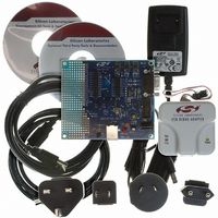
Manufacturer Part Number
C8051F326DK
Description
KIT DEV FOR C8051F326/7
Manufacturer
Silicon Laboratories Inc
Type
MCUr
Specifications of C8051F326DK
Contents
Evaluation Board, Power Supply, USB Cables, Adapter and Documentation
Processor To Be Evaluated
C8051F326/F327
Interface Type
USB
Silicon Manufacturer
Silicon Labs
Core Architecture
8051
Silicon Core Number
C8051F326
Silicon Family Name
C8051F32x
Lead Free Status / RoHS Status
Contains lead / RoHS non-compliant
For Use With/related Products
Silicon Laboratories C8051F326, C8051F327
Lead Free Status / Rohs Status
Lead free / RoHS Compliant
Other names
336-1306


7.2.
When a power-down transition or power irregularity causes VDD to drop below V
monitor will drive the RST pin low and hold the CIP-51 in a reset state (see Figure 7.2). When VDD returns
to a level above V
memory contents are not altered by the power-fail reset, it is impossible to determine if VDD dropped
below the level required for data retention. If the PORSF flag reads ‘1’, the data may no longer be valid.
The VDD monitor is enabled after power-on resets; however its defined state (enabled/disabled) is not
altered by any other reset source. For example, if the VDD monitor is enabled and a software reset is per-
formed, the VDD monitor will still be enabled after the reset.
Important Note: The VDD monitor must be enabled before it is selected as a reset source. Selecting the
VDD monitor as a reset source before it is enabled and stabilized will cause a system reset. The procedure
for configuring the VDD monitor as a reset source is shown below:
See Figure 7.2 for VDD monitor timing. See Table 7.1 for complete electrical characteristics of the VDD
monitor.
Bit7:
Bit6:
Bits5–0: Reserved. Read = Variable. Write = don’t care.
VDMEN VDDSTAT Reserved Reserved Reserved Reserved Reserved Reserved
R/W
Bit7
Power-Fail Reset / VDD Monitor
Step 1. Enable the VDD monitor (VDM0CN.7 = ‘1’).
Step 2. Wait for the VDD monitor to stabilize (see Table 7.1 for the VDD Monitor turn-on time).
Step 3. Select the VDD monitor as a reset source (RSTSRC.1 = ‘1’).
VDMEN: VDD Monitor Enable.
This bit turns the VDD monitor circuit on/off. The VDD Monitor cannot generate system
resets until it is also selected as a reset source in register RSTSRC (Figure 7.2). The VDD
Monitor must be allowed to stabilize before it is selected as a reset source. Selecting the
VDD monitor as a reset source before it has stabilized may generate a system reset.
See Table 7.1 for the minimum VDD Monitor turn-on time. The VDD Monitor is enabled fol-
lowing all POR resets.
0: VDD Monitor Disabled.
1: VDD Monitor Enabled.
VDDSTAT: VDD Status.
This bit indicates the current power supply status (VDD Monitor output).
0: VDD is at or below the VDD monitor threshold.
1: VDD is above the VDD monitor threshold.
Bit6
RST
R
SFR Definition 7.1. VDM0CN: VDD Monitor Control
, the CIP-51 will be released from the reset state. Note that even though internal data
Bit5
R
Bit4
R
Rev. 1.1
Bit3
R
Bit2
R
Bit1
R
C8051F326/7
RST
Bit0
R
, the power supply
SFR Address:
Reset Value
Variable
0xFF
59
Related parts for C8051F326DK
Image
Part Number
Description
Manufacturer
Datasheet
Request
R

Part Number:
Description:
SMD/C°/SINGLE-ENDED OUTPUT SILICON OSCILLATOR
Manufacturer:
Silicon Laboratories Inc
Part Number:
Description:
Manufacturer:
Silicon Laboratories Inc
Datasheet:
Part Number:
Description:
N/A N/A/SI4010 AES KEYFOB DEMO WITH LCD RX
Manufacturer:
Silicon Laboratories Inc
Datasheet:
Part Number:
Description:
N/A N/A/SI4010 SIMPLIFIED KEY FOB DEMO WITH LED RX
Manufacturer:
Silicon Laboratories Inc
Datasheet:
Part Number:
Description:
N/A/-40 TO 85 OC/EZLINK MODULE; F930/4432 HIGH BAND (REV E/B1)
Manufacturer:
Silicon Laboratories Inc
Part Number:
Description:
EZLink Module; F930/4432 Low Band (rev e/B1)
Manufacturer:
Silicon Laboratories Inc
Part Number:
Description:
I°/4460 10 DBM RADIO TEST CARD 434 MHZ
Manufacturer:
Silicon Laboratories Inc
Part Number:
Description:
I°/4461 14 DBM RADIO TEST CARD 868 MHZ
Manufacturer:
Silicon Laboratories Inc
Part Number:
Description:
I°/4463 20 DBM RFSWITCH RADIO TEST CARD 460 MHZ
Manufacturer:
Silicon Laboratories Inc
Part Number:
Description:
I°/4463 20 DBM RADIO TEST CARD 868 MHZ
Manufacturer:
Silicon Laboratories Inc
Part Number:
Description:
I°/4463 27 DBM RADIO TEST CARD 868 MHZ
Manufacturer:
Silicon Laboratories Inc
Part Number:
Description:
I°/4463 SKYWORKS 30 DBM RADIO TEST CARD 915 MHZ
Manufacturer:
Silicon Laboratories Inc
Part Number:
Description:
N/A N/A/-40 TO 85 OC/4463 RFMD 30 DBM RADIO TEST CARD 915 MHZ
Manufacturer:
Silicon Laboratories Inc
Part Number:
Description:
I°/4463 20 DBM RADIO TEST CARD 169 MHZ
Manufacturer:
Silicon Laboratories Inc