C8051F326DK Silicon Laboratories Inc, C8051F326DK Datasheet - Page 7
C8051F326DK
Manufacturer Part Number
C8051F326DK
Description
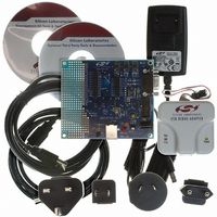
KIT DEV FOR C8051F326/7
Manufacturer
Silicon Laboratories Inc
Type
MCUr
Specifications of C8051F326DK
Contents
Evaluation Board, Power Supply, USB Cables, Adapter and Documentation
Processor To Be Evaluated
C8051F326/F327
Interface Type
USB
Silicon Manufacturer
Silicon Labs
Core Architecture
8051
Silicon Core Number
C8051F326
Silicon Family Name
C8051F32x
Lead Free Status / RoHS Status
Contains lead / RoHS non-compliant
For Use With/related Products
Silicon Laboratories C8051F326, C8051F327
Lead Free Status / Rohs Status
Lead free / RoHS Compliant
Other names
336-1306


List of Figures
1. System Overview
2. Absolute Maximum Ratings
3. Global DC Electrical Characteristics
4. Pinout and Package Definitions
5. Voltage Regulator (REG0)
6. CIP-51 Microcontroller
7. Reset Sources
8. Flash Memory
9. External RAM
10. Oscillators
11. Port Input/Output
12. Universal Serial Bus Controller (USB0)
13. UART0
Figure 1.1. C8051F326 Block Diagram .................................................................... 14
Figure 1.2. C8051F327 Block Diagram .................................................................... 15
Figure 1.3. Typical Connections for the C8051F326................................................ 16
Figure 1.4. Typical Connections for the C8051F327................................................ 16
Figure 1.5. Comparison of Peak MCU Execution Speeds ....................................... 17
Figure 1.6. On-Chip Clock and Reset ...................................................................... 18
Figure 1.7. On-Board Memory Map.......................................................................... 19
Figure 1.8. USB Controller Block Diagram............................................................... 20
Figure 1.9. Development/In-System Debug Diagram............................................... 21
Figure 4.1. C8051F326 QFN-28 Pinout Diagram (Top View) .................................. 27
Figure 4.2. C8051F327 QFN-28 Pinout Diagram (Top View) .................................. 28
Figure 4.3. QFN-28 Package Drawing ..................................................................... 29
Figure 4.4. QFN-28 Recommended PCB Land Pattern ........................................... 30
Figure 5.1. REG0 Configuration: USB Bus-Powered ............................................... 32
Figure 5.2. REG0 Configuration: USB Self-Powered ............................................... 32
Figure 5.3. REG0 Configuration: USB Self-Powered, Regulator Disabled .............. 33
Figure 5.4. REG0 Configuration: No USB Connection............................................. 33
Figure 6.1. CIP-51 Block Diagram............................................................................ 35
Figure 6.2. Memory Map .......................................................................................... 41
Figure 7.1. Reset Sources........................................................................................ 57
Figure 7.2. Power-On and VDD Monitor Reset Timing ............................................ 58
Figure 8.1. Flash Program Memory Map and Security Byte .................................... 66
Figure 9.1. External Ram Memory Map ................................................................... 69
Figure 9.2. XRAM Memory Map Expanded View..................................................... 70
Figure 10.1. Oscillator Diagram................................................................................ 71
Figure 11.1. Port I/O Functional Block Diagram ....................................................... 79
Figure 11.2. Port I/O Cell Block Diagram ................................................................. 80
Figure 12.1. USB0 Block Diagram............................................................................ 87
Figure 12.2. USB0 Register Access Scheme........................................................... 90
Figure 12.3. USB FIFO Allocation ............................................................................ 95
Figure 13.1. UART0 Block Diagram ....................................................................... 117
Rev. 1.1
C8051F326/7
7
Related parts for C8051F326DK
Image
Part Number
Description
Manufacturer
Datasheet
Request
R

Part Number:
Description:
SMD/C°/SINGLE-ENDED OUTPUT SILICON OSCILLATOR
Manufacturer:
Silicon Laboratories Inc
Part Number:
Description:
Manufacturer:
Silicon Laboratories Inc
Datasheet:
Part Number:
Description:
N/A N/A/SI4010 AES KEYFOB DEMO WITH LCD RX
Manufacturer:
Silicon Laboratories Inc
Datasheet:
Part Number:
Description:
N/A N/A/SI4010 SIMPLIFIED KEY FOB DEMO WITH LED RX
Manufacturer:
Silicon Laboratories Inc
Datasheet:
Part Number:
Description:
N/A/-40 TO 85 OC/EZLINK MODULE; F930/4432 HIGH BAND (REV E/B1)
Manufacturer:
Silicon Laboratories Inc
Part Number:
Description:
EZLink Module; F930/4432 Low Band (rev e/B1)
Manufacturer:
Silicon Laboratories Inc
Part Number:
Description:
I°/4460 10 DBM RADIO TEST CARD 434 MHZ
Manufacturer:
Silicon Laboratories Inc
Part Number:
Description:
I°/4461 14 DBM RADIO TEST CARD 868 MHZ
Manufacturer:
Silicon Laboratories Inc
Part Number:
Description:
I°/4463 20 DBM RFSWITCH RADIO TEST CARD 460 MHZ
Manufacturer:
Silicon Laboratories Inc
Part Number:
Description:
I°/4463 20 DBM RADIO TEST CARD 868 MHZ
Manufacturer:
Silicon Laboratories Inc
Part Number:
Description:
I°/4463 27 DBM RADIO TEST CARD 868 MHZ
Manufacturer:
Silicon Laboratories Inc
Part Number:
Description:
I°/4463 SKYWORKS 30 DBM RADIO TEST CARD 915 MHZ
Manufacturer:
Silicon Laboratories Inc
Part Number:
Description:
N/A N/A/-40 TO 85 OC/4463 RFMD 30 DBM RADIO TEST CARD 915 MHZ
Manufacturer:
Silicon Laboratories Inc
Part Number:
Description:
I°/4463 20 DBM RADIO TEST CARD 169 MHZ
Manufacturer:
Silicon Laboratories Inc