C8051F326DK Silicon Laboratories Inc, C8051F326DK Datasheet - Page 63
C8051F326DK
Manufacturer Part Number
C8051F326DK
Description
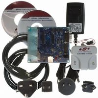
KIT DEV FOR C8051F326/7
Manufacturer
Silicon Laboratories Inc
Type
MCUr
Specifications of C8051F326DK
Contents
Evaluation Board, Power Supply, USB Cables, Adapter and Documentation
Processor To Be Evaluated
C8051F326/F327
Interface Type
USB
Silicon Manufacturer
Silicon Labs
Core Architecture
8051
Silicon Core Number
C8051F326
Silicon Family Name
C8051F32x
Lead Free Status / RoHS Status
Contains lead / RoHS non-compliant
For Use With/related Products
Silicon Laboratories C8051F326, C8051F327
Lead Free Status / Rohs Status
Lead free / RoHS Compliant
Other names
336-1306


8.
On-chip, re-programmable Flash memory is included for program code and non-volatile data storage. The
Flash memory can be programmed in-system, a single byte at a time, through the C2 interface or by soft-
ware using the MOVX instruction. Once cleared to logic 0, a Flash bit must be erased to set it back to logic
1. Flash bytes would typically be erased (set to 0xFF) before being reprogrammed. The write and erase
operations are automatically timed by hardware for proper execution; data polling to determine the end of
the write/erase operation is not required. Code execution is stalled during a Flash write/erase operation.
Refer to Table 8.1 for complete Flash memory electrical characteristics.
8.1.
The simplest means of programming the Flash memory is through the C2 interface using programming
tools provided by Silicon Laboratories or a third party vendor. This is the only means for programming a
non-initialized device. For details on the C2 commands to program Flash memory, see Section “15. C2
Interface” on page 135.
To ensure the integrity of Flash contents, it is strongly recommended that the on-chip VDD Monitor
be enabled in any system that includes code that writes and/or erases Flash memory from soft-
ware.
8.1.1. Flash Lock and Key Functions
Flash writes and erases by user software are protected with a lock and key function. The Flash Lock and
Key Register (FLKEY) must be written with the correct key codes, in sequence, before Flash operations
may be performed. The key codes are: 0xA5, 0xF1. The timing does not matter, but the codes must be
written in order. If the key codes are written out of order, or the wrong codes are written, Flash writes and
erases will be disabled until the next system reset. Flash writes and erases will also be disabled if a Flash
write or erase is attempted before the key codes have been written properly. The Flash lock resets after
each write or erase; the key codes must be written again before a following Flash operation can be per-
formed. The FLKEY register is detailed in Figure 8.2.
8.1.2. Flash Erase Procedure
The Flash memory can be programmed by software using the MOVX write instruction with the address and
data byte to be programmed provided as normal operands. Before writing to Flash memory using MOVX,
Flash write operations must be enabled by: (1) Writing the Flash key codes in sequence to the Flash Lock
register (FLKEY); and (2) Setting the PSWE Program Store Write Enable bit (PSCTL.0) to logic 1 (this
directs the MOVX writes to target Flash memory). The PSWE bit remains set until cleared by software.
A write to Flash memory can clear bits to logic 0 but cannot set them; only an erase operation can set bits
to logic 1 in Flash. A byte location to be programmed must be erased before a new value is written.
The Flash memory is organized in 512-byte pages. The erase operation applies to an entire page (setting
all bytes in the page to 0xFF). To erase an entire 512-byte page, perform the following steps:
Flash Memory
Programming The Flash Memory
Step 1. Disable interrupts (recommended).
Step 2. Write the first key code to FLKEY: 0xA5.
Step 3. Write the second key code to FLKEY: 0xF1.
Step 4. Set the PSEE bit (register PSCTL).
Step 5. Set the PSWE bit (register PSCTL).
Step 6. Using the MOVX instruction, write a data byte to any location within the 512-byte page to
Step 7. Clear the PSWE bit (register PSCTL).
Step 8. Clear the PSEE bit (register PSCTI).
be erased.
Rev. 1.1
C8051F326/7
63
Related parts for C8051F326DK
Image
Part Number
Description
Manufacturer
Datasheet
Request
R

Part Number:
Description:
SMD/C°/SINGLE-ENDED OUTPUT SILICON OSCILLATOR
Manufacturer:
Silicon Laboratories Inc
Part Number:
Description:
Manufacturer:
Silicon Laboratories Inc
Datasheet:
Part Number:
Description:
N/A N/A/SI4010 AES KEYFOB DEMO WITH LCD RX
Manufacturer:
Silicon Laboratories Inc
Datasheet:
Part Number:
Description:
N/A N/A/SI4010 SIMPLIFIED KEY FOB DEMO WITH LED RX
Manufacturer:
Silicon Laboratories Inc
Datasheet:
Part Number:
Description:
N/A/-40 TO 85 OC/EZLINK MODULE; F930/4432 HIGH BAND (REV E/B1)
Manufacturer:
Silicon Laboratories Inc
Part Number:
Description:
EZLink Module; F930/4432 Low Band (rev e/B1)
Manufacturer:
Silicon Laboratories Inc
Part Number:
Description:
I°/4460 10 DBM RADIO TEST CARD 434 MHZ
Manufacturer:
Silicon Laboratories Inc
Part Number:
Description:
I°/4461 14 DBM RADIO TEST CARD 868 MHZ
Manufacturer:
Silicon Laboratories Inc
Part Number:
Description:
I°/4463 20 DBM RFSWITCH RADIO TEST CARD 460 MHZ
Manufacturer:
Silicon Laboratories Inc
Part Number:
Description:
I°/4463 20 DBM RADIO TEST CARD 868 MHZ
Manufacturer:
Silicon Laboratories Inc
Part Number:
Description:
I°/4463 27 DBM RADIO TEST CARD 868 MHZ
Manufacturer:
Silicon Laboratories Inc
Part Number:
Description:
I°/4463 SKYWORKS 30 DBM RADIO TEST CARD 915 MHZ
Manufacturer:
Silicon Laboratories Inc
Part Number:
Description:
N/A N/A/-40 TO 85 OC/4463 RFMD 30 DBM RADIO TEST CARD 915 MHZ
Manufacturer:
Silicon Laboratories Inc
Part Number:
Description:
I°/4463 20 DBM RADIO TEST CARD 169 MHZ
Manufacturer:
Silicon Laboratories Inc