C8051F326DK Silicon Laboratories Inc, C8051F326DK Datasheet - Page 120
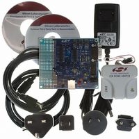
C8051F326DK
Manufacturer Part Number
C8051F326DK
Description
KIT DEV FOR C8051F326/7
Manufacturer
Silicon Laboratories Inc
Type
MCUr
Specifications of C8051F326DK
Contents
Evaluation Board, Power Supply, USB Cables, Adapter and Documentation
Processor To Be Evaluated
C8051F326/F327
Interface Type
USB
Silicon Manufacturer
Silicon Labs
Core Architecture
8051
Silicon Core Number
C8051F326
Silicon Family Name
C8051F32x
Lead Free Status / RoHS Status
Contains lead / RoHS non-compliant
For Use With/related Products
Silicon Laboratories C8051F326, C8051F327
Lead Free Status / Rohs Status
Lead free / RoHS Compliant
Other names
336-1306


C8051F326/7
13.2. Data Format
UART0 has a number of available options for data formatting. Data transfers begin with a start bit (logic
low), followed by the data bits (sent LSB-first), a parity or extra bit (if selected), and end with one or two
stop bits (logic high). The data length is variable between 5 and 8 bits. A parity bit can be appended to the
data, and automatically generated and detected by hardware for even, odd, mark, or space parity. The stop
bit length is selectable between 1 and 2 bit times, and a multi-processor communication mode is available
for implementing networked UART buses. All of the data formatting options can be configured using the
SMOD0 register, shown in SFR Definition 13.2. Figure 13.2 shows the timing for a UART0 transaction
without parity or an extra bit enabled. Figure 13.3 shows the timing for a UART0 transaction with parity
enabled (PE0 = 1). Figure 13.4 is an example of a UART0 transaction when the extra bit is enabled
(XBE0 = 1). Note that the extra bit feature is not available when parity is enabled, and the second stop bit
is only an option for data lengths of 6, 7, or 8 bits.
120
SPACE
SPACE
MARK
MARK
BIT TIMES
BIT TIMES
SPACE
MARK
BIT TIMES
START
START
BIT
BIT
Figure 13.2. UART0 Timing Without Parity or Extra Bit
START
BIT
D
D
Figure 13.4. UART0 Timing With Extra Bit
0
0
Figure 13.3. UART0 Timing With Parity
D
0
D
D
1
1
N bits; N = 5, 6, 7, or 8
N bits; N = 5, 6, 7, or 8
D
1
N bits; N = 5, 6, 7, or 8
Rev. 1.1
D
D
N-2
N-2
D
N-2
D
D
N-1
N-1
D
N-1
PARITY
EXTRA
STOP
BIT 1
STOP
STOP
BIT 1
BIT 1
Optional
(6,7,8 bit
STOP
BIT 2
Data)
Optional
Optional
(6,7,8 bit
(6,7,8 bit
STOP
STOP
BIT 2
Data)
BIT 2
Data)
Related parts for C8051F326DK
Image
Part Number
Description
Manufacturer
Datasheet
Request
R

Part Number:
Description:
SMD/C°/SINGLE-ENDED OUTPUT SILICON OSCILLATOR
Manufacturer:
Silicon Laboratories Inc
Part Number:
Description:
Manufacturer:
Silicon Laboratories Inc
Datasheet:
Part Number:
Description:
N/A N/A/SI4010 AES KEYFOB DEMO WITH LCD RX
Manufacturer:
Silicon Laboratories Inc
Datasheet:
Part Number:
Description:
N/A N/A/SI4010 SIMPLIFIED KEY FOB DEMO WITH LED RX
Manufacturer:
Silicon Laboratories Inc
Datasheet:
Part Number:
Description:
N/A/-40 TO 85 OC/EZLINK MODULE; F930/4432 HIGH BAND (REV E/B1)
Manufacturer:
Silicon Laboratories Inc
Part Number:
Description:
EZLink Module; F930/4432 Low Band (rev e/B1)
Manufacturer:
Silicon Laboratories Inc
Part Number:
Description:
I°/4460 10 DBM RADIO TEST CARD 434 MHZ
Manufacturer:
Silicon Laboratories Inc
Part Number:
Description:
I°/4461 14 DBM RADIO TEST CARD 868 MHZ
Manufacturer:
Silicon Laboratories Inc
Part Number:
Description:
I°/4463 20 DBM RFSWITCH RADIO TEST CARD 460 MHZ
Manufacturer:
Silicon Laboratories Inc
Part Number:
Description:
I°/4463 20 DBM RADIO TEST CARD 868 MHZ
Manufacturer:
Silicon Laboratories Inc
Part Number:
Description:
I°/4463 27 DBM RADIO TEST CARD 868 MHZ
Manufacturer:
Silicon Laboratories Inc
Part Number:
Description:
I°/4463 SKYWORKS 30 DBM RADIO TEST CARD 915 MHZ
Manufacturer:
Silicon Laboratories Inc
Part Number:
Description:
N/A N/A/-40 TO 85 OC/4463 RFMD 30 DBM RADIO TEST CARD 915 MHZ
Manufacturer:
Silicon Laboratories Inc
Part Number:
Description:
I°/4463 20 DBM RADIO TEST CARD 169 MHZ
Manufacturer:
Silicon Laboratories Inc