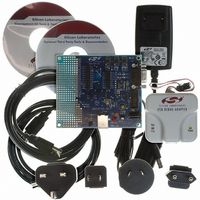
C8051F326DK Silicon Laboratories Inc, C8051F326DK Datasheet - Page 13

C8051F326DK
Manufacturer Part Number
C8051F326DK
Description
KIT DEV FOR C8051F326/7
Manufacturer
Silicon Laboratories Inc
Type
MCUr
Specifications of C8051F326DK
Contents
Evaluation Board, Power Supply, USB Cables, Adapter and Documentation
Processor To Be Evaluated
C8051F326/F327
Interface Type
USB
Silicon Manufacturer
Silicon Labs
Core Architecture
8051
Silicon Core Number
C8051F326
Silicon Family Name
C8051F32x
Lead Free Status / RoHS Status
Contains lead / RoHS non-compliant
For Use With/related Products
Silicon Laboratories C8051F326, C8051F327
Lead Free Status / Rohs Status
Lead free / RoHS Compliant
Other names
336-1306
1.
C8051F326/7 devices are fully integrated mixed-signal system-on-a-chip MCUs. Highlighted features are
listed below. Refer to Table 1.1 for specific product feature selection.
•
•
•
•
•
•
•
•
•
•
•
With on-chip power-on reset, VDD monitor, voltage regulator, and clock oscillator, C8051F326/7 devices
are truly stand-alone System-on-a-Chip solutions. The Flash memory can be reprogrammed in-circuit, pro-
viding non-volatile data storage, and also allowing field upgrades of the 8051 firmware. User software has
complete control of all peripherals, and may individually shut down any or all peripherals for power sav-
ings.
The on-chip Silicon Laboratories 2-Wire (C2) Development Interface allows non-intrusive (uses no on-chip
resources), full speed, in-circuit debugging using the production MCU installed in the final application. This
debug logic supports inspection and modification of memory and registers, setting breakpoints, single
stepping, run and halt commands. All analog and digital peripherals are fully functional while debugging
using C2. The two C2 interface pins can be shared with user functions, allowing in-system debugging with-
out occupying package pins.
Each device is specified for 2.7–5.25 V operation over the industrial temperature range (–40 to +85 °C).
For voltages above 3.6 V, the on-chip Voltage Regulator must be used. A minimum of 3.0 V is required for
USB communication. The Port I/O and RST pins are tolerant of input signals up to 5 V. C8051F326/7 are
available in two 28-pin QFN packages with different pinouts. The RoHS compliant devices are marked with
a -GM suffix in the part number. The port I/O on C8051F326 devices is powered from a separate I/O supply
allowing it to interface to low voltage logic.
High-speed pipelined 8051-compatible microcontroller core (up to 25 MIPS)
In-system, full-speed, non-intrusive debug interface (on-chip)
Universal serial bus (USB) function controller with three fixed-function endpoint pipes, integrated trans-
ceiver, and 256B FIFO RAM
Supply voltage regulator
Precision programmable 12 MHz internal oscillator and 4x clock multiplier
16k kB of on-chip Flash memory
1536 total bytes of on-chip RAM (256 + 1 k + 256 USB FIFO)
Enhanced UART, serial interfaces implemented in hardware
Two general-purpose 16-bit timers
On-chip power-on reset, VDD monitor, and missing clock detector
15 Port I/O (5 V tolerant)
C8051F326-GM
C8051F327-GM
System Overview
25
25
Table 1.1. Product Selection Guide
16k
16k
1536
1536
Rev. 1.1
2
2
C8051F326/7
15
15
—
QFN-28
QFN-28
13


