C8051F326DK Silicon Laboratories Inc, C8051F326DK Datasheet - Page 31
C8051F326DK
Manufacturer Part Number
C8051F326DK
Description
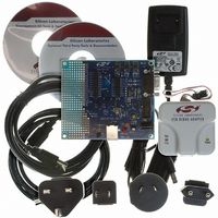
KIT DEV FOR C8051F326/7
Manufacturer
Silicon Laboratories Inc
Type
MCUr
Specifications of C8051F326DK
Contents
Evaluation Board, Power Supply, USB Cables, Adapter and Documentation
Processor To Be Evaluated
C8051F326/F327
Interface Type
USB
Silicon Manufacturer
Silicon Labs
Core Architecture
8051
Silicon Core Number
C8051F326
Silicon Family Name
C8051F32x
Lead Free Status / RoHS Status
Contains lead / RoHS non-compliant
For Use With/related Products
Silicon Laboratories C8051F326, C8051F327
Lead Free Status / Rohs Status
Lead free / RoHS Compliant
Other names
336-1306


5.
C8051F326/7 devices include a voltage regulator (REG0). When enabled, the REG0 output appears on
the VDD pin and can be used to power external devices. REG0 can be enabled/disabled by software using
bit REGEN in register REG0CN. See Table 5.1 for REG0 electrical characteristics.
The voltage regulator is enabled on reset. When the device is self-powered from a 3V supply net, the reg-
ulator may be disabled in order to save power. Important Note: If the voltage at the regulator input
(REGIN) is greater than the Core Supply Voltage (VDD), the voltage regulator should not be dis-
abled. Otherwise, permanent damage to the device may occur.
Note that the VBUS signal must be connected to the VBUS pin when using the device in a USB network.
The VBUS signal should only be connected to the REGIN pin when operating the device as a bus-powered
function. REG0 configuration options are shown in Figure 5.1 - Figure 5.4.
5.1.
REG0 offers a low power mode intended for use when the device is in suspend mode. In this low power
mode, the REG0 output remains as specified; however the REG0 dynamic performance (response time) is
degraded. See Table 5.1 for normal and low power mode supply current specifications. The REG0 mode
selection is controlled via the REGMOD bit in register REG0CN.
5.2.
When the USB Function Controller is used (see section Section “12. Universal Serial Bus Controller
(USB0)” on page 87), the VBUS signal should be connected to the VBUS pin. The VBSTAT bit (register
REG0CN) indicates the current logic level of the VBUS signal. If enabled, a VBUS interrupt will be gener-
ated when the VBUS signal matches the polarity selected by the VBPOL bit in register REG0CN. The
VBUS interrupt is level-sensitive, and has no associated interrupt pending flag. The VBUS interrupt will be
active as long as the VBUS signal matches the polarity selected by VBPOL. See Table 5.1 for VBUS input
parameters.
Important Note: When USB is selected as a reset source, a system reset will be generated when the
VBUS signal matches the polarity selected by the VBPOL bit. See Section “7. Reset Sources” on page 57
for details on selecting USB as a reset source.
Table 5.1. Voltage Regulator Electrical Specifications
V
Input Voltage Range
Output Voltage
VBUS Detection Input Threshold
Bias Current
Dropout Voltage (V
*Note: The minimum input voltage is 2.70 V or V
DD
= 3.0 V; –40 to +85 °C unless otherwise specified.
Voltage Regulator (REG0)
Regulator Mode Selection
VBUS Detection
Parameter
DO
)*
Output Current = 1 to 100 mA
Normal Mode (REGMOD = ‘0’)
Low Power Mode (REGMOD = ‘1’)
IDD = 1 to 100 mA
DD
Conditions
+ V
Rev. 1.1
DO
(max load), whichever is greater.
Min
2.7
3.0
1.0
—
—
—
C8051F326/7
Typ
3.3
1.8
75
41
—
1
Max
5.25
111
3.6
2.9
61
—
mV/mA
Units
µA
V
V
V
31
Related parts for C8051F326DK
Image
Part Number
Description
Manufacturer
Datasheet
Request
R

Part Number:
Description:
SMD/C°/SINGLE-ENDED OUTPUT SILICON OSCILLATOR
Manufacturer:
Silicon Laboratories Inc
Part Number:
Description:
Manufacturer:
Silicon Laboratories Inc
Datasheet:
Part Number:
Description:
N/A N/A/SI4010 AES KEYFOB DEMO WITH LCD RX
Manufacturer:
Silicon Laboratories Inc
Datasheet:
Part Number:
Description:
N/A N/A/SI4010 SIMPLIFIED KEY FOB DEMO WITH LED RX
Manufacturer:
Silicon Laboratories Inc
Datasheet:
Part Number:
Description:
N/A/-40 TO 85 OC/EZLINK MODULE; F930/4432 HIGH BAND (REV E/B1)
Manufacturer:
Silicon Laboratories Inc
Part Number:
Description:
EZLink Module; F930/4432 Low Band (rev e/B1)
Manufacturer:
Silicon Laboratories Inc
Part Number:
Description:
I°/4460 10 DBM RADIO TEST CARD 434 MHZ
Manufacturer:
Silicon Laboratories Inc
Part Number:
Description:
I°/4461 14 DBM RADIO TEST CARD 868 MHZ
Manufacturer:
Silicon Laboratories Inc
Part Number:
Description:
I°/4463 20 DBM RFSWITCH RADIO TEST CARD 460 MHZ
Manufacturer:
Silicon Laboratories Inc
Part Number:
Description:
I°/4463 20 DBM RADIO TEST CARD 868 MHZ
Manufacturer:
Silicon Laboratories Inc
Part Number:
Description:
I°/4463 27 DBM RADIO TEST CARD 868 MHZ
Manufacturer:
Silicon Laboratories Inc
Part Number:
Description:
I°/4463 SKYWORKS 30 DBM RADIO TEST CARD 915 MHZ
Manufacturer:
Silicon Laboratories Inc
Part Number:
Description:
N/A N/A/-40 TO 85 OC/4463 RFMD 30 DBM RADIO TEST CARD 915 MHZ
Manufacturer:
Silicon Laboratories Inc
Part Number:
Description:
I°/4463 20 DBM RADIO TEST CARD 169 MHZ
Manufacturer:
Silicon Laboratories Inc