C8051F326DK Silicon Laboratories Inc, C8051F326DK Datasheet - Page 128
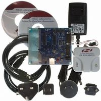
C8051F326DK
Manufacturer Part Number
C8051F326DK
Description
KIT DEV FOR C8051F326/7
Manufacturer
Silicon Laboratories Inc
Type
MCUr
Specifications of C8051F326DK
Contents
Evaluation Board, Power Supply, USB Cables, Adapter and Documentation
Processor To Be Evaluated
C8051F326/F327
Interface Type
USB
Silicon Manufacturer
Silicon Labs
Core Architecture
8051
Silicon Core Number
C8051F326
Silicon Family Name
C8051F32x
Lead Free Status / RoHS Status
Contains lead / RoHS non-compliant
For Use With/related Products
Silicon Laboratories C8051F326, C8051F327
Lead Free Status / Rohs Status
Lead free / RoHS Compliant
Other names
336-1306


C8051F326/7
14.1.1. Mode 0: 13-bit Timer
Timer 0 and Timer 1 operate as 13-bit timers in Mode 0. The following describes the configuration and
operation of Timer 0. However, both timers operate identically, and Timer 1 is configured in the same man-
ner as described for Timer 0.
The TH0 register holds the eight MSBs of the 13-bit timer. TL0 holds the five LSBs in bit positions TL0.4-
TL0.0. The three upper bits of TL0 (TL0.7-TL0.5) are indeterminate and should be masked out or ignored
when reading. As the 13-bit timer register increments and overflows from 0x1FFF (all ones) to 0x0000, the
timer overflow flag TF0 (TCON.5) is set and an interrupt will occur if Timer 0 interrupts are enabled.
Setting the TR0 bit (TCON.4) enables the timer when either GATE0 (TMOD.3) is logic 0 or GATE0 is logic
1 and the input signal /INT0 is active. Setting GATE0 to logic 1 allows the timer to be controlled by the
external input signal /INT0, facilitating pulse width measurements. When GATE0 is set to logic 1, the /INT0
input pin is P0.2.
See Table 6.4 on page 49 for detailed information on how GATE0 affects /INT0 functionality.
Setting TR0 does not force the timer to reset. The timer registers should be loaded with the desired initial
value before the timer is enabled. TL1 and TH1 form the 13-bit register for Timer 1 in the same manner as
described above for TL0 and TH0. Timer 1 is configured and controlled using the relevant TCON and
TMOD bits just as with Timer 0. The input signal /INT1 is used with Timer 1. See Section “6.3.2. External
Interrupts” on page 49 for a complete description of /INT0 and /INT1.
128
G
A
T
E
1
C
T
1
/
M
T
1
1
TMOD
M
T
1
0
G
A
T
E
0
C
T
0
/
M
T
0
1
M
T
0
0
Pre-scaled Clock
SYSCLK
TR0
X = Don't Care
GATE0
0
1
1
1
/INT0
Figure 14.1. T0 Mode 0 Block Diagram
CKCON
Table 14.2. Timer 0 Operation
GATE0
M
T
1
TR0
T
M
0
1
0
X
0
1
1
S
C
A
1
C
S
A
0
Rev. 1.1
0 (P0.2 High)
1 (P0.2 Low)
/INT0
X
X
TCLK
(5 bits)
TL0
Disabled
Disabled
Enabled
Enabled
Timer
(8 bits)
TH0
TR1
TR0
TF1
TF0
IE1
IE0
IT1
IT0
Interrupt
Related parts for C8051F326DK
Image
Part Number
Description
Manufacturer
Datasheet
Request
R

Part Number:
Description:
SMD/C°/SINGLE-ENDED OUTPUT SILICON OSCILLATOR
Manufacturer:
Silicon Laboratories Inc
Part Number:
Description:
Manufacturer:
Silicon Laboratories Inc
Datasheet:
Part Number:
Description:
N/A N/A/SI4010 AES KEYFOB DEMO WITH LCD RX
Manufacturer:
Silicon Laboratories Inc
Datasheet:
Part Number:
Description:
N/A N/A/SI4010 SIMPLIFIED KEY FOB DEMO WITH LED RX
Manufacturer:
Silicon Laboratories Inc
Datasheet:
Part Number:
Description:
N/A/-40 TO 85 OC/EZLINK MODULE; F930/4432 HIGH BAND (REV E/B1)
Manufacturer:
Silicon Laboratories Inc
Part Number:
Description:
EZLink Module; F930/4432 Low Band (rev e/B1)
Manufacturer:
Silicon Laboratories Inc
Part Number:
Description:
I°/4460 10 DBM RADIO TEST CARD 434 MHZ
Manufacturer:
Silicon Laboratories Inc
Part Number:
Description:
I°/4461 14 DBM RADIO TEST CARD 868 MHZ
Manufacturer:
Silicon Laboratories Inc
Part Number:
Description:
I°/4463 20 DBM RFSWITCH RADIO TEST CARD 460 MHZ
Manufacturer:
Silicon Laboratories Inc
Part Number:
Description:
I°/4463 20 DBM RADIO TEST CARD 868 MHZ
Manufacturer:
Silicon Laboratories Inc
Part Number:
Description:
I°/4463 27 DBM RADIO TEST CARD 868 MHZ
Manufacturer:
Silicon Laboratories Inc
Part Number:
Description:
I°/4463 SKYWORKS 30 DBM RADIO TEST CARD 915 MHZ
Manufacturer:
Silicon Laboratories Inc
Part Number:
Description:
N/A N/A/-40 TO 85 OC/4463 RFMD 30 DBM RADIO TEST CARD 915 MHZ
Manufacturer:
Silicon Laboratories Inc
Part Number:
Description:
I°/4463 20 DBM RADIO TEST CARD 169 MHZ
Manufacturer:
Silicon Laboratories Inc