C8051F326DK Silicon Laboratories Inc, C8051F326DK Datasheet - Page 94
C8051F326DK
Manufacturer Part Number
C8051F326DK
Description
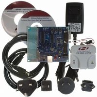
KIT DEV FOR C8051F326/7
Manufacturer
Silicon Laboratories Inc
Type
MCUr
Specifications of C8051F326DK
Contents
Evaluation Board, Power Supply, USB Cables, Adapter and Documentation
Processor To Be Evaluated
C8051F326/F327
Interface Type
USB
Silicon Manufacturer
Silicon Labs
Core Architecture
8051
Silicon Core Number
C8051F326
Silicon Family Name
C8051F32x
Lead Free Status / RoHS Status
Contains lead / RoHS non-compliant
For Use With/related Products
Silicon Laboratories C8051F326, C8051F327
Lead Free Status / Rohs Status
Lead free / RoHS Compliant
Other names
336-1306


C8051F326/7
12.4. USB Clock Configuration
USB0 is capable of communication as a Full or Low Speed USB function. Communication speed is
selected via the SPEED bit in SFR USB0XCN. When operating as a Low Speed function, the USB0 clock
must be 6 MHz. When operating as a Full Speed function, the USB0 clock must be 48 MHz. Clock options
are described in Section “10. Oscillators” on page 71. The USB0 clock is selected via SFR CLKSEL (see
Figure 10.5 on Page 77). The USB transceiver must be enabled before enabling Clock Recovery.
Clock Recovery circuitry uses the incoming USB data stream to adjust the internal oscillator; this allows
the internal oscillator (and 4x Clock Multiplier) to meet the requirements for USB clock tolerance. Clock
Recovery should be used in the following configurations:
When operating USB0 as a Low Speed function with Clock Recovery, software must write ‘1’ to the
CRLOW bit to enable Low Speed Clock Recovery. Clock Recovery is typically not necessary in Low Speed
mode.
Single Step Mode can be used to help the Clock Recovery circuitry to lock when high noise levels are pres-
ent on the USB network. This mode is not required (or recommended) in typical USB environments.
94
Bit7:
Bit6:
Bit5:
Bits4–0: Reserved. Read = Variable. Must Write = 01001b.
CRE
R/W
Bit7
Communication Speed
USB Register Definition 12.5. CLKREC: Clock Recovery Control
CRE: Clock Recovery Enable.
This bit enables/disables the USB clock recovery feature.
0: Clock recovery disabled.
1: Clock recovery enabled.
CRSSEN: Clock Recovery Single Step.
This bit forces the oscillator calibration into ‘single-step’ mode during clock recovery.
0: Normal calibration mode.
1: Single step mode.
CRLOW: Low Speed Clock Recovery Mode.
This bit must be set to ‘1’ if clock recovery is used when operating as a Low Speed USB
device.
0: Full Speed Mode.
1: Low Speed Mode.
CRSSEN
R/W
Low Speed
Bit6
Full Speed
CRLOW
R/W
Bit5
R/W
Bit4
Internal Oscillator/2
4x Clock Multiplier
USB Clock
Rev. 1.1
R/W
Bit3
Reserved
R/W
Bit2
4x Clock Multiplier Input
R/W
Internal Oscillator
Bit1
N/A
R/W
Bit0
USB Address:
00001001
Reset Value
0x0F
Related parts for C8051F326DK
Image
Part Number
Description
Manufacturer
Datasheet
Request
R

Part Number:
Description:
SMD/C°/SINGLE-ENDED OUTPUT SILICON OSCILLATOR
Manufacturer:
Silicon Laboratories Inc
Part Number:
Description:
Manufacturer:
Silicon Laboratories Inc
Datasheet:
Part Number:
Description:
N/A N/A/SI4010 AES KEYFOB DEMO WITH LCD RX
Manufacturer:
Silicon Laboratories Inc
Datasheet:
Part Number:
Description:
N/A N/A/SI4010 SIMPLIFIED KEY FOB DEMO WITH LED RX
Manufacturer:
Silicon Laboratories Inc
Datasheet:
Part Number:
Description:
N/A/-40 TO 85 OC/EZLINK MODULE; F930/4432 HIGH BAND (REV E/B1)
Manufacturer:
Silicon Laboratories Inc
Part Number:
Description:
EZLink Module; F930/4432 Low Band (rev e/B1)
Manufacturer:
Silicon Laboratories Inc
Part Number:
Description:
I°/4460 10 DBM RADIO TEST CARD 434 MHZ
Manufacturer:
Silicon Laboratories Inc
Part Number:
Description:
I°/4461 14 DBM RADIO TEST CARD 868 MHZ
Manufacturer:
Silicon Laboratories Inc
Part Number:
Description:
I°/4463 20 DBM RFSWITCH RADIO TEST CARD 460 MHZ
Manufacturer:
Silicon Laboratories Inc
Part Number:
Description:
I°/4463 20 DBM RADIO TEST CARD 868 MHZ
Manufacturer:
Silicon Laboratories Inc
Part Number:
Description:
I°/4463 27 DBM RADIO TEST CARD 868 MHZ
Manufacturer:
Silicon Laboratories Inc
Part Number:
Description:
I°/4463 SKYWORKS 30 DBM RADIO TEST CARD 915 MHZ
Manufacturer:
Silicon Laboratories Inc
Part Number:
Description:
N/A N/A/-40 TO 85 OC/4463 RFMD 30 DBM RADIO TEST CARD 915 MHZ
Manufacturer:
Silicon Laboratories Inc
Part Number:
Description:
I°/4463 20 DBM RADIO TEST CARD 169 MHZ
Manufacturer:
Silicon Laboratories Inc