C8051F326DK Silicon Laboratories Inc, C8051F326DK Datasheet - Page 8
C8051F326DK
Manufacturer Part Number
C8051F326DK
Description
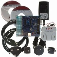
KIT DEV FOR C8051F326/7
Manufacturer
Silicon Laboratories Inc
Type
MCUr
Specifications of C8051F326DK
Contents
Evaluation Board, Power Supply, USB Cables, Adapter and Documentation
Processor To Be Evaluated
C8051F326/F327
Interface Type
USB
Silicon Manufacturer
Silicon Labs
Core Architecture
8051
Silicon Core Number
C8051F326
Silicon Family Name
C8051F32x
Lead Free Status / RoHS Status
Contains lead / RoHS non-compliant
For Use With/related Products
Silicon Laboratories C8051F326, C8051F327
Lead Free Status / Rohs Status
Lead free / RoHS Compliant
Other names
336-1306


C8051F32x-DK
6.3. Universal Serial Bus (USB) Interface (J14)
A Universal Serial Bus (USB) connector (J14) is provided to facilitate connections to the USB interface on the
C8051F320. Table 2 shows the J14 pin definitions.
6.4. Expansion I/O Connector (J1)
The 32-pin Expansion I/O connector J1 provides access to all signal pins of the C8051F320 device. Pins for +3 V,
digital ground and the output of an on-board low-pass filter are also available. A small through-hole prototyping
area is also provided. All I/O signals routed to connector J1 are also routed to through-hole connection points
between J1 and the prototyping area (see Figure 2 on page 6). Each connection point is labeled indicating the
signal available at the connection point. See Table 3 for a list of pin descriptions for J1.
6.5. USB Self-powered Configuration (J2, J11)
The C8051F320 target board can be configured as a self-powered USB device to take power from the USB cable
instead of the ac/dc adapter connected at P1. To configure the target boards as a self-powered USB device,
remove the shorting block from J2 and install on J11. (A shorting block should only be installed on J2 or J11, never
both at the same time.) Install shorting blocks in the following manner:
Note: When the C8051F320 target board is self-powered from the USB, the Serial Adapter is not powered from the
target board. The Serial Adapter must be powered directly by connecting the ac/dc adapter to the Serial Adapters’
dc power jack. Also, the RS232 Serial Interface (J5) cannot be used when powering the target board from the USB.
8
J2(ON) & J11(OFF)
J2(OFF) & J11(ON)
Pin #
10
12
11
1
2
3
4
5
6
7
8
9
+3 VD (+3.3 VDC)
Description
PWM Output
P0.0
P0.1
P0.2
P0.3
P0.4
P0.5
P0.6
P0.7
P1.0
P1.1
→
→
Target Board is powered from the ac/dc Adapter at P1.
Target Board is powered from the USB connection
Table 2. USB Connector Pin Descriptions
Pin #
1
2
3
4
Table 3. J1 Pin Descriptions
Pin #
13
14
15
16
17
18
19
20
21
22
23
24
Rev. 0.8
Description
GND (Ground)
Description
P1.2
P1.3
P1.4
P1.5
P1.6
P1.7
P2.0
P2.1
P2.2
P2.3
P2.4
P2.5
VBUS
D+
D-
Pin #
25
26
27
28
29
30
31
32
GND (Ground)
Description
/RST (Reset)
VREGIN
VBUS
P2.6
P2.7
P3.0
VDD
Related parts for C8051F326DK
Image
Part Number
Description
Manufacturer
Datasheet
Request
R

Part Number:
Description:
SMD/C°/SINGLE-ENDED OUTPUT SILICON OSCILLATOR
Manufacturer:
Silicon Laboratories Inc
Part Number:
Description:
Manufacturer:
Silicon Laboratories Inc
Datasheet:
Part Number:
Description:
N/A N/A/SI4010 AES KEYFOB DEMO WITH LCD RX
Manufacturer:
Silicon Laboratories Inc
Datasheet:
Part Number:
Description:
N/A N/A/SI4010 SIMPLIFIED KEY FOB DEMO WITH LED RX
Manufacturer:
Silicon Laboratories Inc
Datasheet:
Part Number:
Description:
N/A/-40 TO 85 OC/EZLINK MODULE; F930/4432 HIGH BAND (REV E/B1)
Manufacturer:
Silicon Laboratories Inc
Part Number:
Description:
EZLink Module; F930/4432 Low Band (rev e/B1)
Manufacturer:
Silicon Laboratories Inc
Part Number:
Description:
I°/4460 10 DBM RADIO TEST CARD 434 MHZ
Manufacturer:
Silicon Laboratories Inc
Part Number:
Description:
I°/4461 14 DBM RADIO TEST CARD 868 MHZ
Manufacturer:
Silicon Laboratories Inc
Part Number:
Description:
I°/4463 20 DBM RFSWITCH RADIO TEST CARD 460 MHZ
Manufacturer:
Silicon Laboratories Inc
Part Number:
Description:
I°/4463 20 DBM RADIO TEST CARD 868 MHZ
Manufacturer:
Silicon Laboratories Inc
Part Number:
Description:
I°/4463 27 DBM RADIO TEST CARD 868 MHZ
Manufacturer:
Silicon Laboratories Inc
Part Number:
Description:
I°/4463 SKYWORKS 30 DBM RADIO TEST CARD 915 MHZ
Manufacturer:
Silicon Laboratories Inc
Part Number:
Description:
N/A N/A/-40 TO 85 OC/4463 RFMD 30 DBM RADIO TEST CARD 915 MHZ
Manufacturer:
Silicon Laboratories Inc
Part Number:
Description:
I°/4463 20 DBM RADIO TEST CARD 169 MHZ
Manufacturer:
Silicon Laboratories Inc