MPC8313E-RDB Freescale Semiconductor, MPC8313E-RDB Datasheet - Page 11
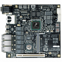
MPC8313E-RDB
Manufacturer Part Number
MPC8313E-RDB
Description
BOARD PROCESSOR
Manufacturer
Freescale Semiconductor
Series
PowerQUICC II™ PROr
Type
MCUr
Datasheets
1.MPC8313CZQAFFB.pdf
(100 pages)
2.MPC8313E-RDBB.pdf
(52 pages)
3.MPC8313E-RDBB.pdf
(2 pages)
Specifications of MPC8313E-RDB
Contents
Reference Design Board, Software and Documentation
Termination Type
SMD
Supply Voltage Max
1.05V
Tool / Board Applications
Wired Connectivity-LIN, CAN, Ethernet, USB
Mcu Supported Families
POWERQUICC II PRO
Rohs Compliant
Yes
Filter Terminals
SMD
Silicon Manufacturer
Freescale
Silicon Core Number
MPC83xx
Kit Application Type
Communication & Networking
Application Sub Type
Ethernet
Core Architecture
Power Architecture
Silicon Family Name
PowerQUICC II PRO
For Use With/related Products
MPC8313E
Lead Free Status / RoHS Status
Lead free / RoHS Compliant


2.4
The MPC8313E processor uses DDR2 SDRAM as the system memory. The DDR2 interface uses the
SSTL2 driver/receiver and 1.8 V power. A Vref 1.8 V/2 is needed for all SSTL2 receivers in the DDR2
interface. For details on DDR2 timing design and termination, refer to the Freescale application note
entitled “Hardware and Layout Design Considerations for DDR Memory Interfaces” (AN2582). Signal
integrity test results show this design does not require terminating resistors (series resistor (R
termination resistor (R
DDR2 chips and MPC8313E are connected directly. The interface is 1.8 V provided by an on-board
Freescale Semiconductor
66.666 MHz
133 MHz
33/66 MHz
25 MHz
125 MHz
48 MHz
50 MHz
24 MHz
32.768 KHz
Clock Frequency
DDR2 SDRAM Controller
MPC8313E CLKIN
DDR2 SDRAM
PCI 32-bit slot and MiniPCI
slot
L2 Switch and GBE PHY
eTSEC clock
USB clock
IEEE1588 Clock (TMR_CLK)
ULPI external USB PHY
Real-time clock
T
PowerQUICC™ MPC8313E Reference Design Board (RDB), Rev. 4
)) for the discrete DDR2 devices used. DDR2 supports on-die termination; the
Module
Table 2. Clock Distribution
66.666 MHz oscillator
MPC8313E
MPC8313E
25 MHz oscillator
GBE PHY with PLL
(REVC), or
125 MHz oscillators
(REVB), or
GBE PHY (REVAx)
48 MHz oscillator
50 MHz oscillator/50
MHz VCXO
24 MHz crystal
32.768 KHz crystal
Generated by
The MPC8313E uses CLKIN to generate the
PCI_SYNC_OUT clock signal, which is fed back
on the board through the PCI_SYNC_IN signal
to the internal system PLL. From the power-on
reset configuration, the CSB clock is generated
by the internal PLL and is fed to the e300 core
PLL for generating the e300 core clock. The
CFG_CLKIN_DIV configuration input selects
whether CLKIN or CLKIN/2 is driven on the
PCI_SYNC_OUT signal. The CFG_CLKIN_DIV
is tied to the M66EN input pin.
The DDR memory controller is configured to use
the 2:1 mode CSB to DDR for the DDR interface
(DDR266). The local bus clock uses 1:1 local to
CSB clock, which is configured by hard reset
configuration or SPMR register.
The PCI module uses the PCI_SYNC_IN as its
clock source. The trace length of the
PCI_SYNC_IN to PCI_SYNC_OUT signal is
matched with all PCI clocks on the RDB.
The 25 MHz oscillator provides the clock for the
L2 switch and the GBE PHY
The GTX_CLK125 and SERDES (SGMII) clocks
are provided by external oscillators (or by GBE
PHY in REVAx and REVC boards).
48 MHz is provided for on-chip USB PHY of
MPC8313E
50 MHz is used by the IEEE 1588 module. It can
be an ordinary oscillator or VCXO controlled by
SPI DAC.
24 MHz crystal is used by the ULPI external
USB PHY
32.768 KHz crystal is used by the real-time clock
Description
Board-Level Functions
S
) and
11
Related parts for MPC8313E-RDB
Image
Part Number
Description
Manufacturer
Datasheet
Request
R

Part Number:
Description:
Mpc8313e Powerquicc Ii Pro Processor
Manufacturer:
Freescale Semiconductor, Inc
Datasheet:

Part Number:
Description:
BOARD CPU 8313E VER 2.1
Manufacturer:
Freescale Semiconductor
Datasheet:

Part Number:
Description:
BOARD CPU 8313E VER 2.2
Manufacturer:
Freescale Semiconductor
Datasheet:
Part Number:
Description:
Microprocessors - MPU 8313 REV2.2 PB ENC EXT
Manufacturer:
Freescale Semiconductor
Datasheet:
Part Number:
Description:
Microprocessors - MPU 8313 REV2.2 PB W/ENC
Manufacturer:
Freescale Semiconductor
Datasheet:
Part Number:
Description:
Microprocessors - MPU 8313 REV2.2 PB NO EN EXT
Manufacturer:
Freescale Semiconductor
Datasheet:
Part Number:
Description:
Microprocessors - MPU 8313 REV2.2 PB NO ENC
Manufacturer:
Freescale Semiconductor
Datasheet:
Part Number:
Description:
Manufacturer:
Freescale Semiconductor, Inc
Datasheet:
Part Number:
Description:
Manufacturer:
Freescale Semiconductor, Inc
Datasheet:
Part Number:
Description:
Manufacturer:
Freescale Semiconductor, Inc
Datasheet:
Part Number:
Description:
Manufacturer:
Freescale Semiconductor, Inc
Datasheet:
Part Number:
Description:
Manufacturer:
Freescale Semiconductor, Inc
Datasheet:
Part Number:
Description:
Manufacturer:
Freescale Semiconductor, Inc
Datasheet:
Part Number:
Description:
Manufacturer:
Freescale Semiconductor, Inc
Datasheet:
Part Number:
Description:
Manufacturer:
Freescale Semiconductor, Inc
Datasheet: