P0304 Terasic Technologies Inc, P0304 Datasheet - Page 70
P0304
Manufacturer Part Number
P0304
Description
DE2-70 CALL FOR ACADEMIC PRICING
Manufacturer
Terasic Technologies Inc
Type
FPGAr
Datasheet
1.P0304.pdf
(93 pages)
Specifications of P0304
Contents
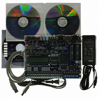
DE2-70 Board, Power Supply, Cables, Plastic cover and software
For Use With/related Products
Cyclone II 2C70
For Use With
P0033 - BOARD ADAPTER HSMC TO GPIOP0006 - BOARD ADAPTER THDB-SUMP0001 - MODULE DIGITAL CAMERA 5MP (D5M)P0307 - KIT DEV 4.3" LCD TOUCH PANEL
Lead Free Status / RoHS Status
Lead free / RoHS Compliant
Other names
DE2-70
Available stocks
Company
Part Number
Manufacturer
Quantity
Price
Company:

Part Number:
P0304UAL
Manufacturer:
Littelfuse
Quantity:
45 000
Company:
Part Number:
P0304UBL
Manufacturer:
Littelfuse
Quantity:
45 000
Company:
Part Number:
P0304UCL
Manufacturer:
Littelfuse
Quantity:
45 000


The Verilog source code for this demonstration is provided in the DE2_70_Default folder, which
also includes the necessary files for the corresponding Quartus II project. The top-level Verilog file,
called DE2_70_Default.v, can be used as a template for other projects, because it defines ports that
correspond to all of the user-accessible pins on the Cyclone II FPGA.
6.2 TV Box Demonstration
This demonstration plays video and audio input from a DVD player using the VGA output, audio
CODEC, and one TV decoder (U11) on the DE2-70 board. Figure 6.1 shows the block diagram of
the design. There are two major blocks in the circuit, called I2C_AV_Config and TV_to_VGA. The
TV_to_VGA block consists of the ITU-R 656 Decoder, SDRAM Frame Buffer, YUV422 to YUV444,
YCrCb to RGB, and VGA Controller. The figure also shows the TV Decoder (ADV7180) and the
VGA DAC (ADV7123) chips used.
As soon as the bit stream is downloaded into the FPGA, the register values of the TV Decoder chip
are used to configure the TV decoder via the I2C_AV_Config block, which uses the I2C protocol to
communicate with the TV Decoder chip. Following the power-on sequence, the TV Decoder chip
will be unstable for a time period; the Lock Detector is responsible for detecting this instability.
The ITU-R 656 Decoder block extracts YCrCb 4:2:2 (YUV 4:2:2) video signals from the ITU-R 656
data stream sent from the TV Decoder. It also generates a data valid control signal indicating the
valid period of data output. Because the video signal from the TV Decoder is interlaced, we need to
perform de-interlacing on the data source. We used the SDRAM Frame Buffer and a field selection
multiplexer(MUX) which is controled by the VGA controller to perform the de-interlacing operation.
Internally, the VGA Controller generates data request and odd/even selected signals to the SDRAM
Frame Buffer and filed selection multiplexer(MUX). The YUV422 to YUV444 block converts the
selected YCrCb 4:2:2 (YUV 4:2:2) video data to the YCrCb 4:4:4 (YUV 4:4:4) video data format.
Finally, the YCrCb_to_RGB block converts the YCrCb data into RGB output. The VGA Controller
block generates standard VGA sync signals VGA_HS and VGA_VS to enable the display on a VGA
Optionally connect a VGA display to the VGA D-SUB connector. When connected, the
Optionally connect a powered speaker to the stereo audio-out jack
Place toggle switch SW17 in the UP position to hear a 1 kHz humming sound from the
VGA display should show a pattern of colors
audio-out port. Alternatively, if switch SW17 is DOWN, the microphone-in port can be
connected to a microphone to hear voice sounds, or the line-in port can be used to play audio
from an appropriate sound source
67
DE2-70 User Manual
Related parts for P0304
Image
Part Number
Description
Manufacturer
Datasheet
Request
R

Part Number:
Description:
MODULE DIGITAL CAMERA 5MP (D5M)
Manufacturer:
Terasic Technologies Inc
Datasheet:

Part Number:
Description:
USB BLASTER CABLE
Manufacturer:
Terasic Technologies Inc
Datasheet:

Part Number:
Description:
BOARD ADAPTER HSMC TO GPIO
Manufacturer:
Terasic Technologies Inc
Datasheet:

Part Number:
Description:
BOARD ADAPTER THDB-SUM
Manufacturer:
Terasic Technologies Inc
Datasheet:

Part Number:
Description:
KIT DEV 4.3" LCD TOUCH PANEL
Manufacturer:
Terasic Technologies Inc
Datasheet:

Part Number:
Description:
DAUGHTER BOARD AD/DA GPIO ADA
Manufacturer:
Terasic Technologies Inc

Part Number:
Description:
DAUGHTER BOARD AD/DA HSMC ADA
Manufacturer:
Terasic Technologies Inc

Part Number:
Description:
KIT MAX II MICRO
Manufacturer:
Terasic Technologies Inc
Datasheet:

Part Number:
Description:
BOARD DEV/EDUCATION ALTERA DE0
Manufacturer:
Terasic Technologies Inc
Datasheet:

Part Number:
Description:
BOARD DEV DE1 ALTERA
Manufacturer:
Terasic Technologies Inc
Datasheet:

Part Number:
Description:
DE2 CALL FOR ACADEMIC PRICING
Manufacturer:
Terasic Technologies Inc

Part Number:
Description:
MODULE DIGITAL CAMERA 1.3MP
Manufacturer:
Terasic Technologies Inc
Datasheet:

Part Number:
Description:
SENSOR CMOS 1.3MEGA (FOR P0349)
Manufacturer:
Terasic Technologies Inc
Datasheet:
Part Number:
Description:
MODULE DIGITAL CAMERA 5MP (D5M)
Manufacturer:
Terasic Technologies Inc
Datasheet: