CY8CKIT-020 Cypress Semiconductor Corp, CY8CKIT-020 Datasheet - Page 61
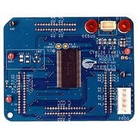
CY8CKIT-020
Manufacturer Part Number
CY8CKIT-020
Description
KIT PSOC CY8C28 FAMILY PROCESSOR
Manufacturer
Cypress Semiconductor Corp
Series
PSoC®r
Type
MCUr
Specifications of CY8CKIT-020
Contents
Board, Software and Documentation
Silicon Manufacturer
Cypress
Core Architecture
PSoC
Features
Programmable System-on-chip Design Methodology And Architecture
Kit Contents
PSoC CY8C28 Module, Doc, CD
Silicon Core Number
CY8C28
Silicon Family Name
PSoC
Rohs Compliant
Yes
Lead Free Status / RoHS Status
Lead free / RoHS Compliant
For Use With/related Products
CY8C28 Family
Lead Free Status / Rohs Status
Supplier Unconfirmed
Other names
428-3036


2.1.6.2
2.1.6.3
2.1.6.4
CY8CKIT-020 PSoC Development Kit Guide, Doc. # 001-56971 Rev. **
SW4 - Processor Reset Button
The board has a push button switch that resets the PSoC device attached to the processor module.
One side of the switch is tied to the XRES pin of the processor module socket. The other end of the
switch is tied to the HW_RESET pin of the processor module socket. Doing this allows the module
designer to tie the HW_RESET line either high or low, depending on which direction the processor
reset is active.
Note PSoC 1 devices are active high reset. Therefore, a light pull-down resistor may be necessary
on the XRES pin of designs with these devices to avoid unintentional device resets. PSoC 3 and
PSoC 5 devices are active low reset. Therefore, a light pull-up resistor may be necessary on the
XRES pin of designs with these devices to avoid unintentional device resets.
U8 - External MHz Oscillator
The board supports the use of an external high frequency 8-pin PDIP oscillator. The speed of the
oscillator supported is dependent on the specifications of the PSoC device used. The output of this
oscillator is routed to P15_4 on receptacle P2 and TP62 near P2 of the DVK board.
P1, P2, P3 and P4 - Processor Module Receptacles
Processor modules provide modularity to this board. Sockets P1-P4 are used to connect a proces-
sor module to the board. All supported GPIOs (including special I/Os), along with VDD DIG, VDD
ANLG, 5V, 3.3V, VBUS and VBAT (only connected to a surface mount pad on the board) are con-
nected to these receptacles. In addition, each of the VDDIO power pins are connected to these
receptacles. The full speed USB D+ and D- signals are also connected to one of the sockets. Pro-
cessor reset is connected to P1. Any "no connect" pins are brought out to surface mount test pads.
Table 2-4. Connector Pin Assignments - Processor Module Sockets
Pin Number
10
11
12
13
14
15
16
17
18
19
20
1
2
3
4
5
6
7
8
9
GND
VDDD
V5_0
GND
VBAT
DM
V3_3
DP
VBUS
VDDIO1
P5_6
P5_7
P5_4
P5_5
P12_6
P12_7
P1_6
P1_7
P1_4
P1_5
P1 (West)
GND
GND
P6_1
P6_0
P6_3
P6_2
P15_5
P15_4
P9_2
P9_0
P2_1
P2_0
P2_3
P2_2
VDDIO2
P9_3
P2_5
P2_4
P2_7
P2_6
P2 (North)
GND
GND
P12_2
P12_3
P8_0
P8_1
P4_0
P4_1
P8_2
P8_3
P0_0
P0_1
P0_2
P0_3
VDDIO0
VDDA
P0_4
P0_5
P0_6
P0_7
P3 (East)
GND
P7_7
NC7
NC8
NC5
NC6
NC3
NC4
P7_6
P7_5
P12_0
P12_1
P3_6
P3_7
P7_4
VDDIO3
P3_4
P3_5
P3_2
P3_3
P4 (South)
Board Specifications and Layout
61
Related parts for CY8CKIT-020
Image
Part Number
Description
Manufacturer
Datasheet
Request
R

Part Number:
Description:
KIT DEV FOR PSOC3/5
Manufacturer:
Cypress Semiconductor Corp
Datasheet:

Part Number:
Description:
PSoC1/3/5 Development Kit
Manufacturer:
Cypress Semiconductor Corp
Datasheet:

Part Number:
Description:
KIT DEV PSOC PROC MODULE CY8C38
Manufacturer:
Cypress Semiconductor Corp

Part Number:
Description:
KIT DEV PSOC PROC MODULE CY8C29
Manufacturer:
Cypress Semiconductor Corp

Part Number:
Description:
KIT DEV PSOC ANALOG VOLTMETER
Manufacturer:
Cypress Semiconductor Corp
Datasheet:

Part Number:
Description:
KIT DEV PSOC5 FIRST TOUCH
Manufacturer:
Cypress Semiconductor Corp
Datasheet:

Part Number:
Description:
KIT DEV PSOC3 FIRSTTOUCH STARTER
Manufacturer:
Cypress Semiconductor Corp
Datasheet:
Part Number:
Description:
KIT DEV PROC MODULE PSOC5
Manufacturer:
Cypress Semiconductor Corp
Datasheet:

Part Number:
Description:
KIT PSOC MINIPROG3 PROGRAM DEBUG
Manufacturer:
Cypress Semiconductor Corp
Datasheet:

Part Number:
Description:
DEV KIT PSOC 5 CY8C55
Manufacturer:
Cypress Semiconductor Corp
Datasheet:

Part Number:
Description:
KIT EVAL POWERLINE HIGH VOLT
Manufacturer:
Cypress Semiconductor Corp
Datasheet:

Part Number:
Description:
KIT PSOC FIRST TOUCH
Manufacturer:
Cypress Semiconductor Corp
Datasheet:

Part Number:
Description:
EVAL KIT WORLDTOUR2
Manufacturer:
Cypress Semiconductor Corp
Datasheet:

Part Number:
Description:
KIT UNIVERSAL CAPSENSE CTRLR
Manufacturer:
Cypress Semiconductor Corp
Datasheet: