MC56F8006DEMO Freescale Semiconductor, MC56F8006DEMO Datasheet - Page 16
MC56F8006DEMO
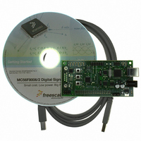
Manufacturer Part Number
MC56F8006DEMO
Description
DEMO BOARD FOR MC56F8006
Manufacturer
Freescale Semiconductor
Type
DSPr
Datasheets
1.MC56F8006DEMO.pdf
(13 pages)
2.MC56F8006DEMO.pdf
(8 pages)
3.MC56F8006DEMO.pdf
(2 pages)
4.MC56F8006DEMO.pdf
(100 pages)
Specifications of MC56F8006DEMO
Contents
Board
Processor To Be Evaluated
MC56F8006
Interface Type
RS-232, USB
Operating Supply Voltage
3.3 V
Silicon Manufacturer
Freescale
Core Architecture
56800/E
Core Sub-architecture
56800/E
Silicon Core Number
MC56F
Silicon Family Name
MC56F80xx
Rohs Compliant
Yes
For Use With/related Products
MC56F8006
Lead Free Status / RoHS Status
Lead free / RoHS Compliant


Signal/Connection Descriptions
4.3
After reset, each pin is configured for its primary function (listed first). Any alternate functionality must be programmed via the
GPIO module’s peripheral enable registers (GPIO_x_PER) and SIM module’s (GPS_xn) GPIO peripheral select registers. If
CLKIN or XTAL is selected as device external clock input, the CLK_MOD bit in the OCCS oscillator control register (OSCTL)
needs to be set too. EXT_SEL bit in OSCTL selects CLKIN or XTAL.
16
GPIOB6/RXD/SDA/ANA13 & CMP0_P2/CLKIN
ANB8 and PGA1+ & CMP0_M2/GPIOC4
ANB6 and PGA1– & CMP0_P4/GPIOC5
GPIOB7/TXD/SCL/ANA11 & CMP2_M3
GPIOB1/SS/SDA/ANA12 & CMP2_P3
ANB4 & CMP1_P1/GPIOC6/PWM2
56F8006/56F8002 Signal Pins
GPIOC7/ANB5 & CMP1_M2
GPIOE2/ANB7 & CMP0_M1
GPIOE1/ANB9 & CMP0_P1
GPIOB5/T1/FAULT3/SCLK
Figure 6. Top View, MC56F8006 48-Pin LQFP Package
GPIOE0
MC56F8006/MC56F8002 Digital Signal Controller, Rev. 3
V
DDA
1
2
3
4
5
6
7
8
9
10
11
12
Orientation Mark
36
35
34
33
32
31
30
29
28
27
26
25
GPIOA3/PWM3/TXD/EXTAL
GPIOA2/PWM2
GPIOA4/PWM4/SDA/FAULT1/TIN2
GPIOB0/SCLK/SCL/ANB13/PWM3/T1
GPIOE6
GPIOB4/T0/CLKO_0/MISO/SDA/RXD/ANA0 & ANB0
GPIOE7/CMP1_M3
V
GPIOA5/PWM5/FAULT2 or EXT_SYNC/TIN3
Vss
GPIOA6/FAULT0/ANA1 & ANB1/SCL/TXD/CLKO_1
GPIOB2/MISO/TIN2/ANA2 & ANB2/CMP0_OUT
DD
Freescale Semiconductor
Related parts for MC56F8006DEMO
Image
Part Number
Description
Manufacturer
Datasheet
Request
R

Part Number:
Description:
Manufacturer:
Freescale Semiconductor, Inc
Datasheet:
Part Number:
Description:
Manufacturer:
Freescale Semiconductor, Inc
Datasheet:
Part Number:
Description:
Manufacturer:
Freescale Semiconductor, Inc
Datasheet:
Part Number:
Description:
Manufacturer:
Freescale Semiconductor, Inc
Datasheet:
Part Number:
Description:
Manufacturer:
Freescale Semiconductor, Inc
Datasheet:
Part Number:
Description:
Manufacturer:
Freescale Semiconductor, Inc
Datasheet:
Part Number:
Description:
Manufacturer:
Freescale Semiconductor, Inc
Datasheet:
Part Number:
Description:
Manufacturer:
Freescale Semiconductor, Inc
Datasheet:
Part Number:
Description:
Manufacturer:
Freescale Semiconductor, Inc
Datasheet:
Part Number:
Description:
Manufacturer:
Freescale Semiconductor, Inc
Datasheet:
Part Number:
Description:
Manufacturer:
Freescale Semiconductor, Inc
Datasheet:
Part Number:
Description:
Manufacturer:
Freescale Semiconductor, Inc
Datasheet:
Part Number:
Description:
Manufacturer:
Freescale Semiconductor, Inc
Datasheet:
Part Number:
Description:
Manufacturer:
Freescale Semiconductor, Inc
Datasheet:
Part Number:
Description:
Manufacturer:
Freescale Semiconductor, Inc
Datasheet: